Detailed description – Rainbow Electronics MAX867 User Manual
Page 7
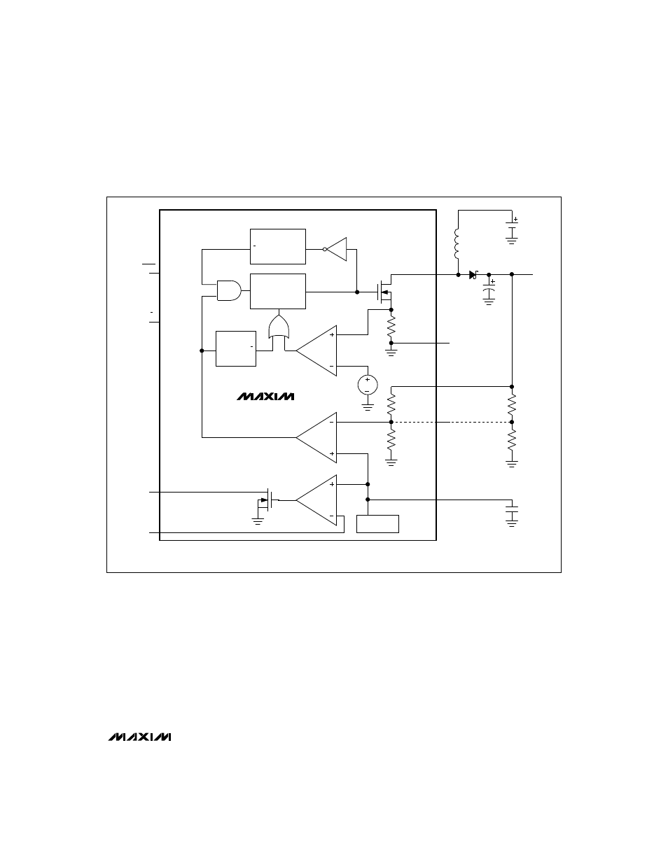
_______________Detailed Description
Operating Principle
The MAX866/MAX867 combine a switch-mode regula-
tor, N-channel power MOSFET, precision voltage refer-
ence, and power-fail detector in a single monolithic
device. The MOSFET is a “sense-FET” type for best effi-
ciency, and has a very low gate threshold voltage to
ensure start-up with low battery voltages (0.8V typ).
PFM Control Scheme
The MAX866/MAX867 control scheme (Figure 1) com-
bines low-voltage efficiency (80% typ) with low battery
drain (100µA typ). There is no oscillator; switching is
accomplished by a pair of one shots that set a maxi-
mum LX on-time (4.5µs typ) and a minimum LX off-time
(1µs). LX on-time will be terminated early if the inductor
current reaches 0.5A before 4.5µs elapses. With the
standard application circuit (Figure 2a), LX current is
typically less than 50mA, so LX on-time is normally not
terminated by the 0.5A limit and lasts the complete
4.5µs. The LX on-resistance is typically 1
Ω
to minimize
switch losses. The MAX866/MAX867 switching frequen-
cy depends on load, input voltage, and inductor value,
and it can range up to 250kHz with typical component
values.
MAX866/MAX867
3.3V/5V or Adjustable-Output,
Single-Cell DC-DC Converters
_______________________________________________________________________________________
7
MAX866/MAX867
SHDN
3/5*
LBO
LBI
N
LBI COMPARATOR
ERROR COMPARATOR
CURRENT-LIMIT
COMPARATOR
ONE-SHOT
TRIG
Q
Q
ONE-SHOT
TRIG
S
Q
R
F/F
MINIMUM
OFF-TIME
ONE-SHOT
V
BATT
LX
N
GND
OUT
V
OUT
**
FB**
**
*
*
REF
REFERENCE
MAXIMUM
ON-TIME
ONE-SHOT
*MAX866 ONLY
**MAX867 ONLY
Figure 1. Block Diagram