Rainbow Electronics MAX867 User Manual
Page 2
V
MAX866/MAX867
3.3V/5V or Adjustable-Output,
Single-Cell DC-DC Converters
2
_______________________________________________________________________________________
ABSOLUTE MAXIMUM RATINGS
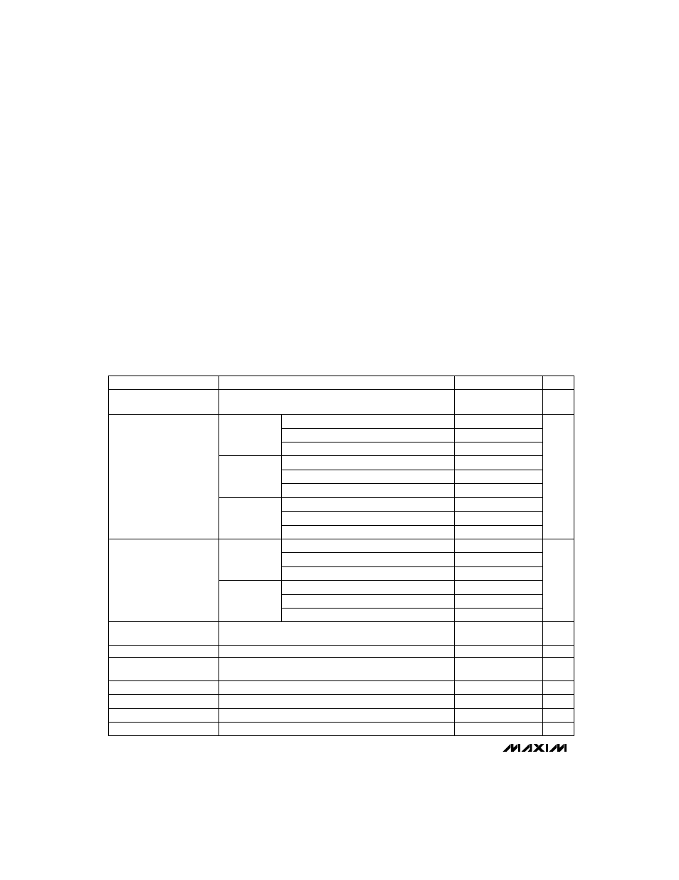
ELECTRICAL CHARACTERISTICS
(Circuit of Figure 2, V
IN
= 1.2V, I
LOAD
= 0mA, T
A
= +25°C, unless otherwise noted.)
Stresses beyond those listed under “Absolute Maximum Ratings” may cause permanent damage to the device. These are stress ratings only, and functional
operation of the device at these or any other conditions beyond those indicated in the operational sections of the specifications is not implied. Exposure to
absolute maximum rating conditions for extended periods may affect device reliability.
Supply Voltage (OUT to GND) ...................................-0.3V, +7V
Switch Voltage (LX to GND) .......................................-0.3V, +7V
S
—
H
—
D
—
N
–
, LBO to GND ....................................................-0.3V, +7V
LBI, REF, 3/
–
5
–
, FB to GND ............................-0.3V, (V
OUT
+ 0.3V)
Reference Current (I
REF
) ..................................................2.5mA
Continuous Power Dissipation (T
A
= +70°C)
SO (derate 5.88mW/°C above +70°C) .........................471mW
µMAX (derate 4.1mW/°C above +70°C) ......................330mW
Reverse Battery Current (T
A
≤
+45°C) (Note 1) ................750mA
Operating Temperature Ranges
MAX86_C/D .......................................................0°C to +70°C
MAX86_E_A ....................................................-40°C to +85°C
Junction Temperature .....................................................+150°C
Storage Temperature Range ............................-65°C to +160°C
Lead Temperature (soldering, 10sec) ............................+300°C
Note 1:
Reverse battery current is measured from the
Typical Operating Circuit’s
battery input terminal to GND when the battery is
connected backwards. A reverse current of 750mA will not exceed the package dissipation limits but, if left for an extended
time (more than ten minutes), may degrade performance.
With falling edge
3/
–
5
–
= 3V, -20µA
≤
REF load
≤
250µA, C
REF
= 0.22µF
No REF load
0.9V
≤
V
IN
≤
3V
I
LOAD
= 0mA, 3/
–
5
–
= 3V, LBI = 1.5V,
V
OUT
= 3.47V, FB = 1.5V
CONDITIONS
V
1.22
1.25
1.28
LBI Input Threshold
%
0.8
2.0
Reference Load Regulation
V
1.22
1.25
1.28
Reference Voltage
mA
500
µA
1
Shutdown Quiescent Current
(Note 4)
µA
27
60
Quiescent Supply Current in
3.3V mode (Note 4)
4.80
5.0
5.20
3.17
3.3
3.43
4.80
5.0
5.20
4.75
5.0
5.25
3.13
3.3
3.47
4.75
5.0
5.25
Output Voltage
(Note 2)
UNITS
MIN
TYP
MAX
PARAMETER
Peak Inductor Current Limit
MAX866, 3/
–
5
–
= 0V, 0mA
≤
I
LOAD
≤
6mA
MAX866, 3/
–
5
–
= 3V, 0mA
≤
I
LOAD
≤
8mA
MAX867, V
OUT
= 5V, 0mA
≤
I
LOAD
≤
6mA
MAX866, 3/
–
5
–
= 0V, 0mA
≤
I
LOAD
≤
6mA
MAX866, 3/
–
5
–
= 3V, 0mA
≤
I
LOAD
≤
8mA
MAX867, V
OUT
= 5V, 0mA
≤
I
LOAD
≤
6mA
S
—
H
—
D
—
N
–
= 0V, 3/
–
5
–
= 3V, LBI = 1.5V, V
OUT
= 3.47V,
FB = 1.5V
0.9V
≤
V
IN
≤
3V
MAX866, 3/
–
5
–
= 0V, 4.8V
≤
V
LOAD
≤
5.2V
MAX866, 3/
–
5
–
= 3V, 3.17V
≤
V
LOAD
≤
3.43V
MAX867, V
OUT
= 5V, 4.8V
≤
V
LOAD
≤
5.2V
MAX866, 3/
–
5
–
= 0V, 4.8V
≤
V
LOAD
≤
5.2V
MAX866, 3/
–
5
–
= 3V, 3.17V
≤
V
LOAD
≤
3.43V
MAX867, V
OUT
= 5V, 4.8V
≤
V
LOAD
≤
5.2V
6
9
8
13
6
9
10
15
15
23
mA
10
15
Maximum Load Current
(Note 2)
0.9V
≤
V
IN
≤
3V,
T
A =
T
MIN TO
T
MAX
(Note 3)
1.2V
≤
V
IN
≤
3V
V
0.8
0.9
Minimum Start-Up
Supply Voltage
Output set for 3.3V, measured at V
IN
in Figure 2, V
IN
= 1.5V
µA
100
No-Load Battery Current
1.2V
≤
V
IN
≤
3V
MAX866, 3/
–
5
–
= 0V, 0mA
≤
I
LOAD
≤
10mA
MAX866, 3/
–
5
–
= 3V, 0mA
≤
I
LOAD
≤
15mA
MAX867, V
OUT
= 5V, 0mA
≤
I
LOAD
≤
10mA
4.80
5.0
5.20
3.17
3.3
3.43
4.80
5.0
5.20