Detailed description, Applications information – Rainbow Electronics MAX3627 User Manual
Page 9

MAX3627
+3.3V, Low-Jitter, Precision Clock
Generator with Multiple Outputs
_______________________________________________________________________________________
9
Detailed Description
The MAX3627 is a frequency generator designed to
operate at Ethernet frequencies. It consists of an on-
chip crystal oscillator, PLL, LVCMOS output buffer, and
LVDS output buffers. Using a low-frequency clock
(crystal or CMOS input) as a reference, the internal PLL
generates a high-frequency output clock with excellent
jitter performance. The outputs can be switched among
125MHz, 156.25MHz, and 312.5MHz.
Crystal Oscillator
An integrated oscillator provides the low-frequency ref-
erence clock for the PLL. This oscillator requires an
external crystal connected between X_IN and X_OUT.
The crystal frequency is 25MHz. See the
Applications
Information
section for more information.
OSC_IN Buffer
The LVCMOS OSC_IN buffer is internally biased to
allow AC- or DC-coupling. This input is internally AC-
coupled, and is designed to operate at 25MHz when
the PLL is enabled (PLL_BP is left open). When the PLL
is bypassed (PLL_BP is set low), the OSC_IN buffer can
be operated from 20MHz to 320MHz.
PLL
The PLL takes the signal from the crystal oscillator or
reference clock input and synthesizes a low-jitter, high-
frequency clock. The PLL contains a phase-frequency
detector (PFD), a lowpass filter, and a voltage-con-
trolled oscillator (VCO) that operates at 625MHz. The
PLL bandwidth is tuned to 150kHz typical to optimize
both phase noise and power-supply noise rejection
(PSNR). The VCO output is connected to the PFD input
through a feedback divider that divides the VCO fre-
quency by 25 to lock onto the 25MHz reference clock
or oscillator. For output Q0, the FSELA pin is used to
select among 125MHz, 156.25MHz, and 312.5MHz. For
outputs Q1 to Q6, the FSELB pin is used to select
among 125MHz, 156.25MHz, and 312.5MHz. For the
Q7 output, the FSELB pin is used to select between
125MHz and 156.25MHz. To minimize the jitter induced
by power-supply noise, the VCO supply (V
DDA
) is iso-
lated from the core logic and output buffer supplies.
LVDS Drivers
The high-frequency outputs—Q0, Q1, Q2, Q3, Q4, Q5,
and Q6—are differential LVDS buffers designed to
drive 100
Ω.
LVCMOS Driver
LVCMOS output Q7 is provided on the MAX3627. It is
designed to drive single-ended high-impedance loads.
The output specifications are only valid up to 160MHz.
Applications Information
Power-Supply Filtering
The MAX3627 is a mixed analog/digital IC. The PLL
contains analog circuitry susceptible to random noise.
To take full advantage of on-board filtering and noise
attenuation, in addition to excellent on-chip power-sup-
ply rejection, this part provides a separate power-sup-
ply pin, V
DDA
, for the VCO circuitry. The purpose of this
design technique is to ensure clean input power supply
to the VCO circuitry and to improve the overall immunity
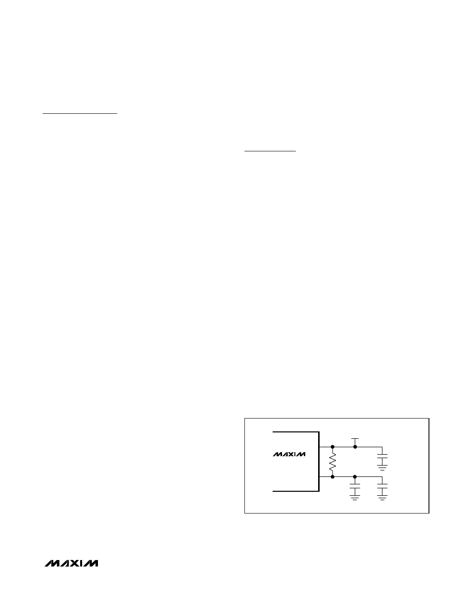
to power-supply noise. Figure 4 illustrates the recom-
mended power-supply filter network for V
DDA
. This net-
work requires that the power supply is +3.3V ±5%.
Decoupling capacitors should be used on all other sup-
ply pins and placed as close as possible to the pins for
best performance.
Crystal Input Layout
and Frequency Stability
The MAX3627 features an integrated on-chip crystal
oscillator to minimize system implementation cost. The
integrated crystal oscillator is a Pierce-type that uses
the crystal in its parallel resonance mode. It is recom-
mended to use a 25MHz crystal with a load specifica-
tion of C
L
= 18pF. See Table 1 for the recommended
crystal specifications.
The crystal, trace, and two external capacitors should
be placed on the board as close as possible to the
X_IN and X_OUT pins to minimize the board parasitic
capacitance and prevent active signals from coupling
into the oscillator.
V
DD
V
DDA
10.5
Ω
+3.3V
±5%
0.01
μF
10
μF
0.1
μF
MAX3627
Figure 4. Analog Supply Filtering
