Electrical characteristics (continued) – Rainbow Electronics MAX3627 User Manual
Page 3

MAX3627
+3.3V, Low-Jitter, Precision Clock
Generator with Multiple Outputs
_______________________________________________________________________________________
3
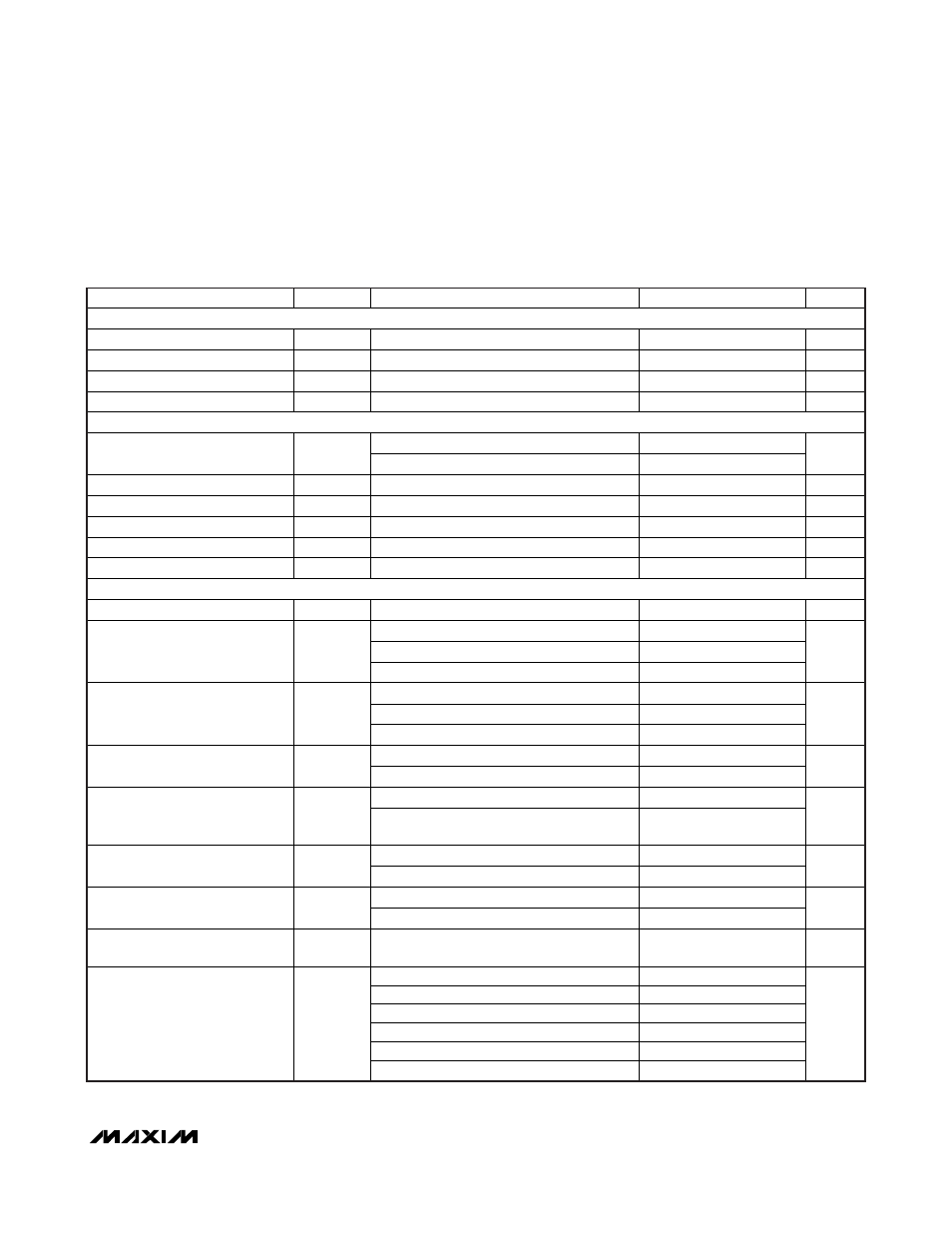
ELECTRICAL CHARACTERISTICS (continued)
(V
DD
= +3.0V to +3.6V, T
A
= 0°C to +70°C, unless otherwise noted. Typical values are at V
DD
= +3.3V, T
A
= +25°C, unless otherwise
noted. When using X_IN, X_OUT input, no signal is applied at OSC_IN. When PLL is enabled, PLL_BP = high-Z or high. When PLL is
bypassed, PLL_BP = low.) (Note 1)
PARAMETER
SYMBOL
CONDITIONS
MIN
TYP
MAX
UNITS
INPUT SPECIFICATIONS (FSELA, FSELB,
PLL_BP, OE)
Input-Voltage High
V
IH
2.0
V
DD
V
Input-Voltage Low
V
IL
0
0.8
V
Input High Current
I
IH
V
IN
= V
DD
80
μA
Input Low Current
I
IL
V
IN
= 0
-80
μA
LVCMOS/LVTTL INPUT SPECIFICATIONS (OSC_IN) (Note 6)
PLL
enabled
25
Input Clock Frequency
PLL bypassed
20
320
MHz
Input Amplitude Range
(Note 7)
1.2
3.6
V
Input High Current
I
IH
V
IN
= V
DD
80
μA
Input Low Current
I
IL
V
IN
= 0
-80
μA
Reference Clock Duty Cycle
40
50
60
%
Input Capacitance
C
IN
1.5
pF
CLOCK OUTPUT AC SPECIFICATIONS
VCO
Center
Frequency
625 MHz
FSELA = GND
125
FSELA = V
DD
156.25
Output Frequency with PLL
Enabled (Q0)
FSELA = high-Z
312.5
MHz
FSELB = GND
125
FSELB = V
DD
156.25
Output Frequency with PLL
Enabled (Q1 to Q7)
FSELB = high-Z (Note 8)
312.5
MHz
LVDS outputs
20
320
Output Frequency with PLL
Disabled
LVCMOS output
20
160
MHz
12kHz to 20MHz,
PLL_BP = high (Note 9)
0.4
1.0
Integrated Phase Jitter
RJ
RMS
12kHz to 20MHz,
PLL_BP = high-Z
(Note 10)
0.4
ps
RMS
LVDS
outputs
-64
Power-Supply Noise Rejection
(Note 11)
PSNR
LVCMOS
output
-49
dBc
LVDS outputs
2.5
Deterministic Jitter Due to
Supply Noise (Note 12)
LVCMOS
output
18
ps
P-P
Nonharmonic and Subharmonic
Spurs
(Note
13)
-70 dBc
f
=
100Hz
-115
f
=
1kHz
-124
f
=
10kHz
-126
f = 100kHz
-130
f
=
1MHz
-143
LVDS Clock Output SSB Phase
Noise at 125MHz (Note 14)
f
>
10MHz
-149
dBc/Hz
