Chip information, Package information – Rainbow Electronics MAX3627 User Manual
Page 11

MAX3627
+3.3V, Low-Jitter, Precision Clock
Generator with Multiple Outputs
Maxim cannot assume responsibility for use of any circuitry other than circuitry entirely embodied in a Maxim product. No circuit patent licenses are
implied. Maxim reserves the right to change the circuitry and specifications without notice at any time.
Maxim Integrated Products, 120 San Gabriel Drive, Sunnyvale, CA 94086 408-737-7600 ____________________ 11
© 2009 Maxim Integrated Products
Maxim is a registered trademark of Maxim Integrated Products, Inc.
Interface Models
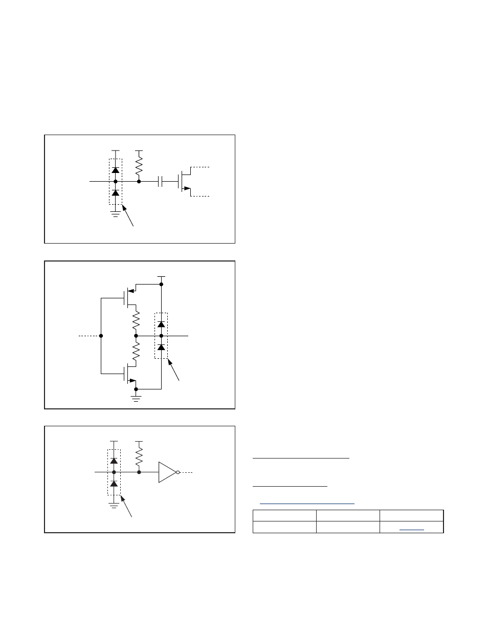
Figures 7, 8, and 9 show examples of interface models.
Layout Considerations
The inputs and outputs are the most critical paths for
the MAX3627 and great care should be taken to mini-
mize discontinuities on these transmission lines
between the connector and the IC. Here are some sug-
gestions for maximizing the performance of the
MAX3627:
• An uninterrupted ground plane should be posi-
tioned beneath the clock outputs. The ground
plane under the crystal should be removed to mini-
mize capacitance.
• Ground pin vias should be placed close to the IC
and the input/output interfaces to allow a return
current path to the MAX3627 and the receive
devices.
• Supply decoupling capacitors should be placed
close to the supply pins, preferably on the same
layer as the MAX3627.
• Take care to isolate crystal input traces from the
MAX3627 outputs.
• The crystal, trace, and two external capacitors
should be placed on the board as close as possi-
ble to the X_IN and X_OUT pins.
• Maintain 100
Ω differential (or 50Ω single-ended)
transmission line impedance into and out of the part.
• Use good high-frequency layout techniques and
multilayer boards with an uninterrupted ground
plane to minimize EMI and crosstalk.
Refer to the MAX3627 evaluation kit for more information.
Exposed-Pad Package
The exposed pad on the 32-pin TQFN package pro-
vides a very low inductance path for return current trav-
eling to the PCB ground plane. The pad is thermal and
electrical ground on the MAX3627 and must be sol-
dered to the circuit board ground for proper electrical
performance.
Chip Information
PROCESS: BiCMOS
180k
Ω
1.4V
ESD
STRUCTURES
OSC_IN
V
DD
Figure 7. Simplified OSC_IN Pin Circuit Schematic
10
Ω
10
Ω
ESD
STRUCTURES
Q7
V
DDO_SE
Figure 8. Simplified LVCMOS Output Circuit Schematic
75k
Ω
ESD
STRUCTURES
OE
V
DD
V
DDO_DIFF
Figure 9. Simplified OE Pin Circuit Schematic
Package Information
For the latest package outline information and land patterns, go
to
www.maxim-ic.com/packages
.
PACKAGE TYPE
PACKAGE CODE
DOCUMENT NO.
32 TQFN-EP
T3255+5
