Typical operating characteristics (continued), Pin description – Rainbow Electronics MAX2645 User Manual
Page 8
MAX2645
3.4GHz to 3.8GHz SiGe
Low-Noise Amplifier/PA Predriver
8
_______________________________________________________________________________________
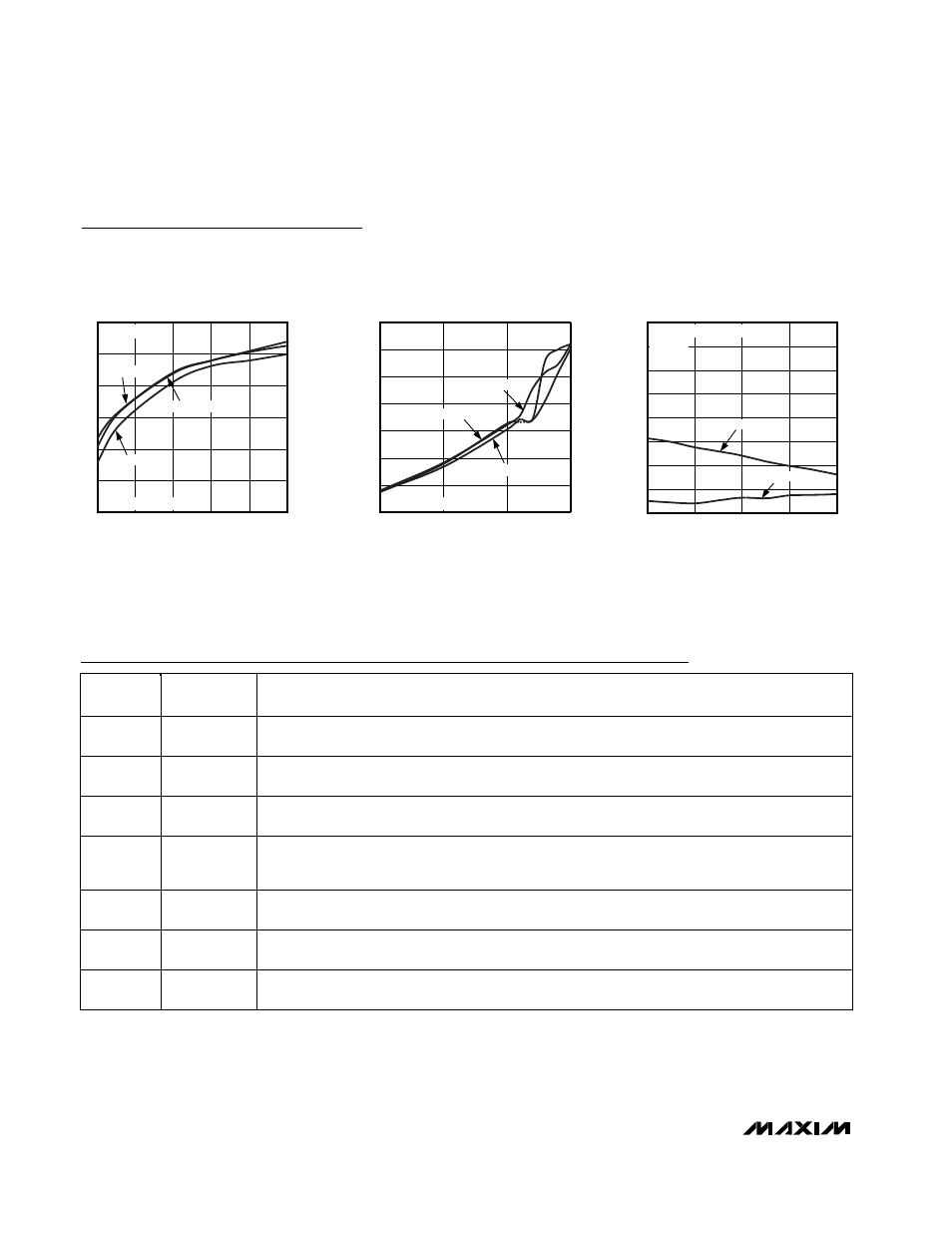
Typical Operating Characteristics (continued)
(MAX2645 EV kit, V
CC
= +3.3V, R
BIAS
= 20k
Ω, f
RFIN
= 3550MHz, T
A
= +25°C, unless otherwise noted.)
7
9
8
11
10
12
13
3.0
4.0
3.5
4.5
5.0
5.5
OUTPUT P1dB POINT vs. SUPPLY VOLTAGE
(HIGH-GAIN MODE)
MAX2645-31
SUPPLY VOLTAGE (V)
T
A
= +25
°C
T
A
= +85
°C
T
A
= -40
°C
PA PREDRIVER CIRCUIT
V
CC
= 5V
-25
-15
-20
-5
-10
5
0
10
-10.0
-5.0
0
5.0
OUTPUT POWER vs. INPUT POWER
(LOW-GAIN MODE)
MAX2645-32
INPUT POWER (dBm)
OUTPUT POWER (dBm)
T
A
= +25°C
T
A
= +85°C
T
A
= -40°C
PA PREDRIVER CIRCUIT
V
CC
= 5V
1.0
1.5
2.0
2.5
3.0
3.5
4.0
4.5
5.0
3.4
3.5
3.6
3.7
3.8
INPUT VSWR vs. FREQUENCY
MAX2645-33
FREQUENCY (GHz)
VSWR
HIGH GAIN
LOW GAIN
PA PREDRIVER CIRCUIT
V
CC
= 5V
Pin Description
PIN
NAME
FUNCTION
1, 2, 4, 7,
EP
GND
Ground. Connect to ground plane with a low-inductance connection. Solder exposed paddle evenly
to the board ground plane.
3
RFIN
RF Input Port to Amplifier. Requires a matching network and a DC-blocking capacitor that may be
part of this network. See Figure 1 for recommended component values.
5
BIAS
Bias-Setting Resistor Connection. A resistor, R
BIAS
, placed from BIAS to ground sets the linearity
and supply current of the amplifier.
6
RFOUT
RF Open-Collector Output Port of Amplifier. Requires a matching network composed of an
inductance to V
CC
and a DC-blocking capacitor. See Figure 1 for recommended component
values.
8
SHDN
Shutdown Control Logic-Level Input. A logic high enables the device for normal operation. A logic
low places the device in low-power shutdown mode.
9
GAIN
Gain Control Logic-Level Input. A logic high places the device in high-gain mode. A logic low
places the device in low-gain mode, reducing the gain by 25dB.
10
V
CC
Power Supply Input. Bypass directly to ground with a capacitor as close to the supply pin as
possible. See Figure 1 for recommended component values.