Rainbow Electronics MAX2645 User Manual
Page 10
RF Output
The RFOUT port is an open-collector output that must be
tied to V
CC
through an inductance for proper biasing.
The MAX2645 EV kit uses a length of transmission line
equivalent to 1.5nH of inductance. A DC-blocking
capacitor is required and can be part of the output
matching network. See Figure 1 for component values
recommended for operation over the 3.4GHz to 3.8GHz
frequency range. See Table 1 for matching to other fre-
quencies. This transmission line is terminated at the
V
CC
node with a radial stub for high-frequency bypass-
ing. This arrangement provides a high-Q, low-loss bias
network used to optimize performance. The radial stub
can be replaced with an appropriate microwave
capacitor.
Power-Supply, Bias Circuitry, and Logic-
Input Bypassing
Proper power-supply bypassing is essential for high-fre-
quency circuit stability. Bypass V
CC
with 10µF, 0.1µF,
and 50pF capacitors located as close to the V
CC
pin as
possible.
To minimize the amount of noise injected into the bias
circuitry and logic inputs, bypass the pins with capaci-
tors located as near to the device pin as possible. For
additional isolation on the logic-control pins, place resis-
tors between the logic-control inputs and the bypass
capacitors. See Figure 1 for recommended component
values; refer to MAX2645 EV kit manual for recommend-
ed board layout.
Layout Considerations
A properly designed PC board is an essential part of any
RF/microwave circuit. Keep RF signal lines as short as
possible to reduce losses, radiation, and inductance.
Use separate, low-inductance vias to the ground plane
for each ground pin. For best performance, solder the
exposed paddle on the bottom of the device package
evenly to the board ground plane.
MAX2645
3.4GHz to 3.8GHz SiGe
Low-Noise Amplifier/PA Predriver
10
______________________________________________________________________________________
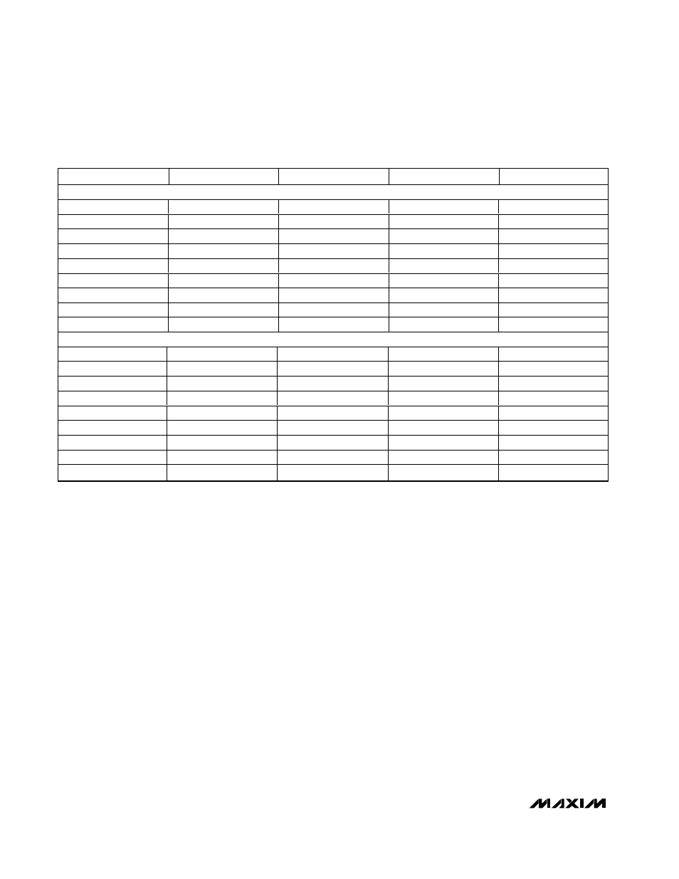
Table 2. MAX2645 Noise Parameters
FREQUENCY (MHz)
FMIN (dB)
|
Γopt|
Γopt ANGLE
RN (
Ω)
R
BIAS
= 20k
Ω, V
CC
= +3.3V, T
A
= +25
°C
3400
2.098
0.237
144.1
31.1
3450
2.122
0.235
146.1
31.5
3500
2.148
0.235
148.2
32.0
3550
2.173
0.234
150.3
32.5
3600
2.198
0.233
152.4
32.9
3650
2.225
0.232
154.5
33.5
3700
2.251
0.231
156.5
33.9
3750
2.279
0.230
158.6
34.5
3800
2.306
0.229
160.7
35.0
R
BIAS
= 15k
Ω, V
CC
= +5V, T
A
= +25
°C
3400
2.103
0.210
146.3
31.1
3450
2.127
0.209
148.4
31.6
3500
2.152
0.208
150.5
32.1
3550
2.177
0.207
152.6
32.5
3600
2.203
0.206
154.7
33.0
3650
2.229
0.206
156.8
33.5
3700
2.256
0.205
158.9
34.0
3750
2.282
0.204
161.0
34.6
3800
2.310
0.204
163.1
35.1