Max2670 gps/gnss front-end amplifier, Detailed description, Layout considerations – Rainbow Electronics MAX2670 User Manual
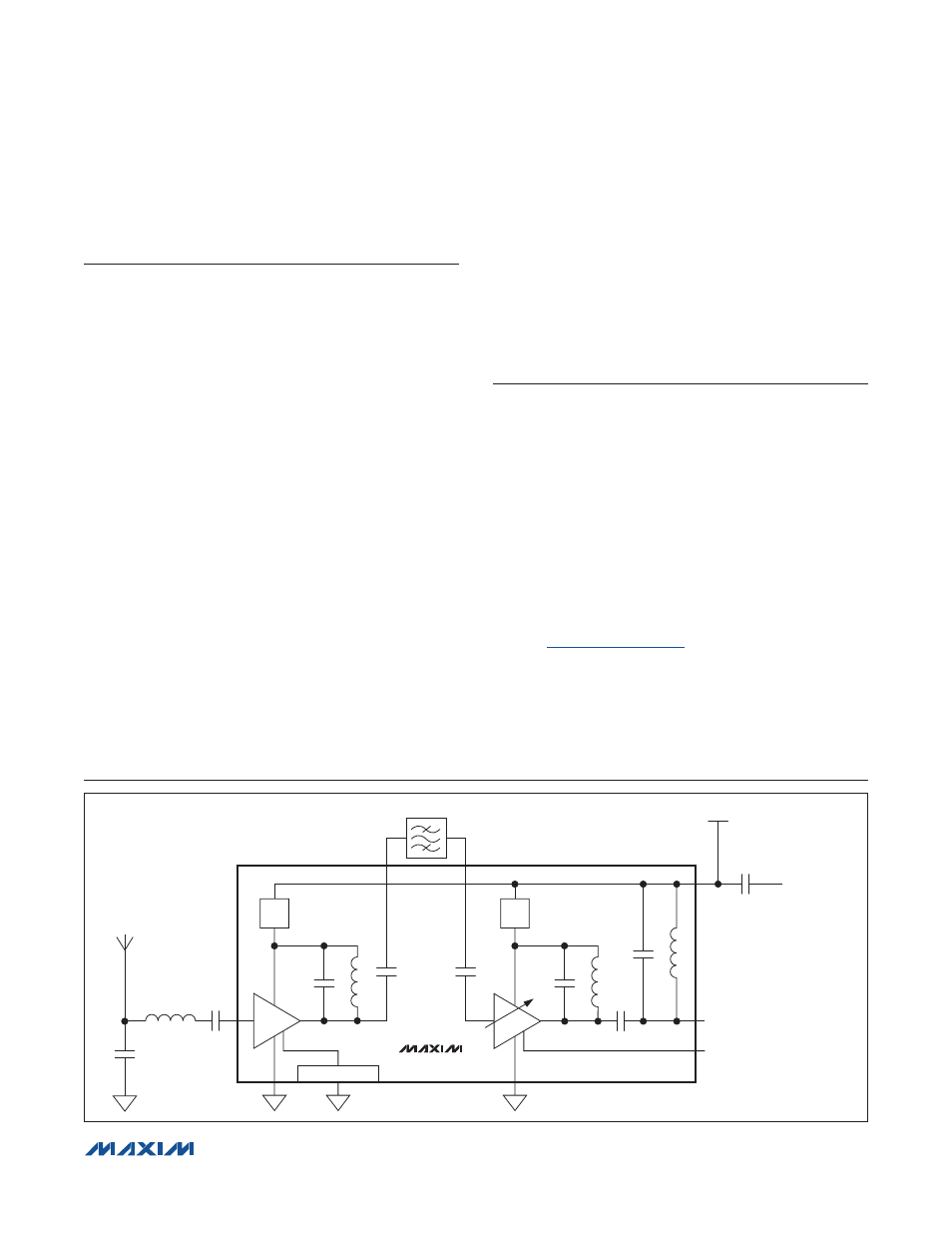
Page 7: Typical operating circuit
����������������������������������������������������������������� Maxim Integrated Products 7
MAX2670
GPS/GNSS Front-End Amplifier
Detailed Description
The MAX2670 IC contains two LNA stages tuned for use
at 1575MHz.
AMP 1
AMP 1 has an internal load that limits the bandwidth and
provides a 50I output impedance through a DC-blocking
capacitor. The internal biasing for AMP 1 suppresses
gain variation with changes in temperature and supply
voltage. At the input, an integrated DC-blocking capaci-
tor and matching network are intentionally omitted to
allow selection of external components to optimize for
noise or gain.
AMP 2 with Gain Step
The output of AMP 2 has the dual role of providing both
the RF output drive and receiving the DC power supply
through a single cable. Both the input and output ports
of AMP 2 are internally matched to 50I impedance at
1575MHz. A 3.4dB gain switch can be used to adjust
the gain for different applications. The gain-select pin is
connected to an inverter with an internal pullup resistor.
Hence, the gain-select pin is set by default to high-gain
mode. Shorting the gain-select pin to ground sets the
gain stage to a 3.4dB lower gain. As with AMP 1, AMP
2 has an internal load that limits the bandwidth, and the
amplifier’s internal biasing suppresses gain variation with
changes in temperature and supply voltage.
Alternate Supply (ALT_VCC)
The IC power can be supplied from the navigation sys-
tem through RFOUT2 (pin 5). An integrated filter is con-
nected to the output of LNA 2 to separate the supply volt-
age from the GPS signal. Alternatively, the supply voltage
can be applied to the external capacitor pin (pin 4).
Layout Considerations
For best performance, carefully lay out the PCB using
high-frequency techniques. Use controlled-impedance
transmission lines to interface with the MAX2670 high-
speed inputs and outputs and isolate the input sig-
nals from the output signals as much as possible. For
improved noise figure, keep the connection to the input
of LNA 1 as short as possible. A power-supply decou-
pling capacitor should be placed very close to pin 4 and
connected directly to a ground plane. If low-gain selec-
tion for LNA 2 is required, connect pin 7 directly to the
ground plane with a very short PCB trace. Good ground-
ing is critical for this device. The backside ground plane
should be as close as possible.
Refer to
www.maxim-ic.com
for the MAX2670 Evaluation
Kit schematic, gerber data, pads layout file and BOM
information.
Typical Operating Circuit
1
LNA2 INPUT
LNA1 INPUT
2/3
4
5
6
7
8/9
10
SAW
V
CC
REG
V
CC
REG
LNA 2
ALT_VCC
RFOUT2/VCC
GAIN_SELECT
OPEN = 31.4dB GAIN
SHORT TO GROUND = 28dB GAIN
EXPOSED PAD
LNA 1
MAX2670