Rainbow Electronics MAX2670 User Manual
Max2670 gps/gnss front-end amplifier, Functional diagram, General description
MAX2670
GPS/GNSS Front-End Amplifier
����������������������������������������������������������������� Maxim Integrated Products 1
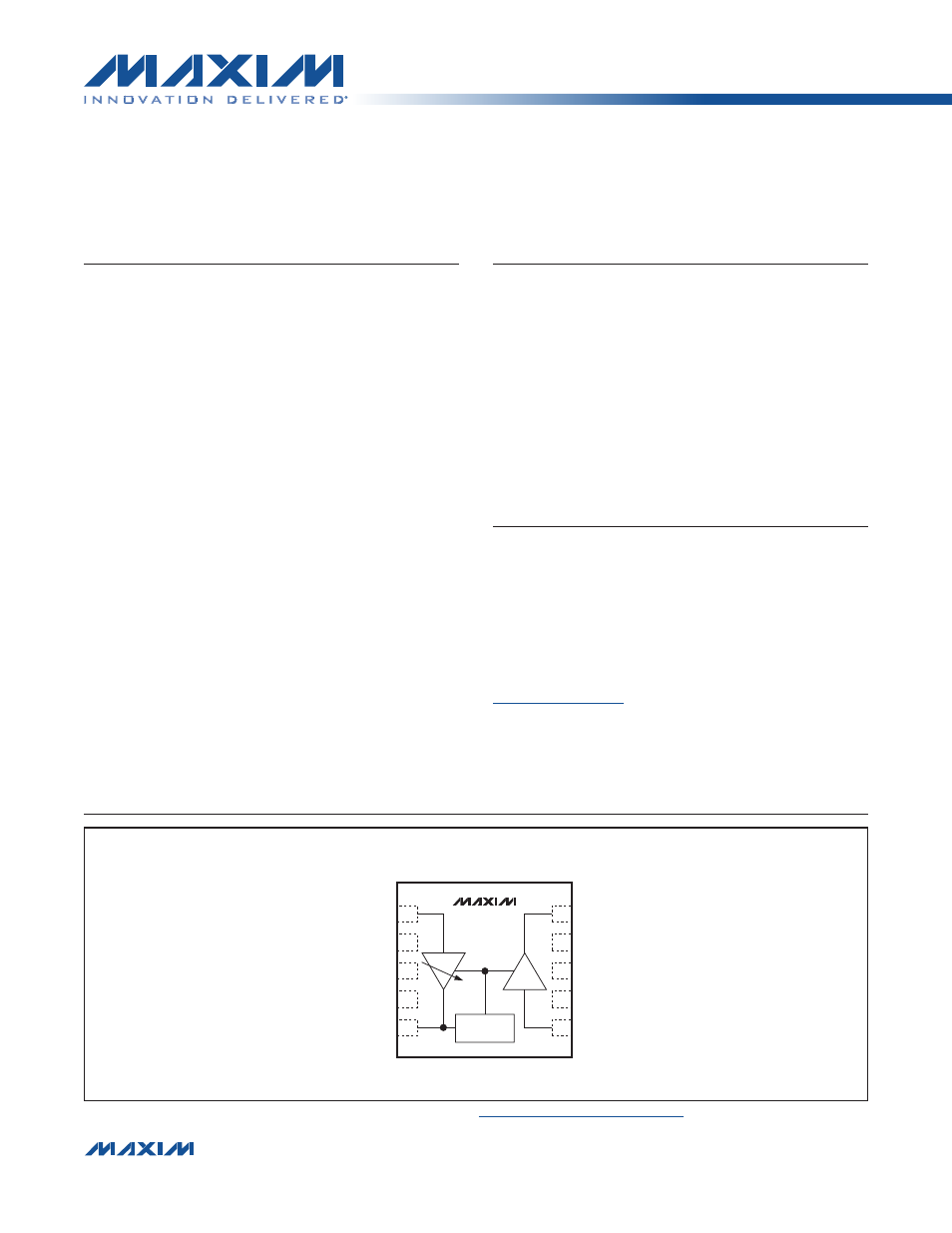
Functional Diagram
Typical Operating Circuit appears at end of data sheet.
19-5655; Rev 0; 6/11
For related parts and recommended products to use with this part, refer to
www.maxim-ic.com/MAX2670.related
.
*Without external input impedance match.
**First amplifier input is impedance matched (S
11
= -10dB).
Second amplifier set to high gain. Amplifiers cascaded without
interstage filter.
E V A L U A T I O N K I T A V A I L A B L E
General Description
The MAX2670 GPS/GNSS front-end amplifier IC is
designed for automotive and marine GPS/GNSS satellite
navigation antenna modules or for any application that
needs to compensate for cable losses from the antenna
to receiver. Two unconditionally stable low-noise amplifier
stages provide the high gain and integrated I/O matching
to minimize the need for external matching components
and eliminate the need for additional gain stages. The
device features the option to place a bandpass ceramic
or SAW filter between the two amplifier stages to provide
a narrow-band output to further improve the noise perfor-
mance of the GPS/GNSS receiver. Additionally, a 3.4dB
gain step is provided to compensate for cable loss varia-
tion between different applications.
The device is designed to operate across all GNSS fre-
quency standards with a 34.8dB typical cascaded gain
and a 25mA supply current. The two LNA stages allow
the use of a wide range of GNSS filter types for maxi-
mum flexibility in system design. The final RF output pin,
which drives the cable to the GNSS receiver, is also the
power-supply connection that accepts a DC supply in
the 3.0V to 5.5V range. Alternatively, the DC supply can
be applied to pin 4.
This GPS/GNSS front-end amplifier is designed on a low-
noise, advanced SiGe process and is available in a lead-
free, 10-pin TDFN surface-mount package (3mm x 3mm).
Features
S
First Amplifier Noise Figure*: 1.0dB
S
High Gain**: 34.8dB
S
3.4dB Gain Step
S
Shared V
CC
and RFOUT2 Pin
S
Integrated 50I Output Matching
S
3.0V to 5.5V Supply Voltage Range
S
Small, Low-Cost Package (3mm x 3mm)
S
AEC-Q100 Qualified
S
ESD Protected to ±2kV Human Body Model
Applications
Integrated Automotive and Marine GPS Receivers
Active Antennas
1
+
3
4
10
8
7
RFOUT1
DC
GENERATION
GND
GAIN_SELECT
RFIN2
GND
EXTCAP/ALT_VCC
2
9
GND
GND
5
6
RFIN1
RFOUT2/VCC
TDFN
TOP VIEW
AMP 2
AMP 1
MAX2670
For pricing, delivery, and ordering information, please contact Maxim Direct at 1-888-629-4642,
or visit Maxim’s website at www.maxim-ic.com.