Hot swap – Rainbow Electronics MAX3033E User Manual
Page 9

Machine Model
The Machine Model for ESD tests all pins using a
200pF storage capacitor and zero discharge resis-
tance. Its objective is to emulate the stress caused by
contact that occurs with handling and assembly during
manufacturing. Of course, all pins require this protec-
tion during manufacturing, not just inputs and outputs.
Therefore, after PC board assembly, the Machine
Model is less relevant to I/O ports.
Hot Swap
When circuit boards are plugged into a “hot” back-
plane, there can be disturbances to the differential sig-
nal levels that could be detected by receivers
connected to the transmission line. This erroneous data
could cause data errors to an RS-422 system. To avoid
this, the MAX3030E–MAX3033E have hot-swap capa-
ble inputs.
When a circuit board is plugged into a “hot” backplane,
there is an interval during which the processor is going
through its power-up sequence. During this time, the
processor’s output drivers are high impedance and are
unable to drive the enable inputs of the MAX3030E–
MAX3033E (EN, EN, EN_) to defined logic levels.
Leakage currents from these high-impedance drivers,
of as much as 10µA, could cause the enable inputs of
the MAX3030E–MAX3033E to drift high or low.
Additionally, parasitic capacitance of the circuit board
could cause capacitive coupling of the enable inputs to
either GND or V
CC
. These factors could cause the
enable inputs of the MAX3030E–MAX3033E to drift to
levels that may enable the transmitter outputs. To avoid
this problem, the hot-swap input provides a method of
holding the enable inputs of the MAX3030E–MAX3033E
in the disabled state as V
CC
ramps up. This hot-swap
input is able to overcome the leakage currents and par-
asitic capacitances that can pull the enable inputs to
the enabled state.
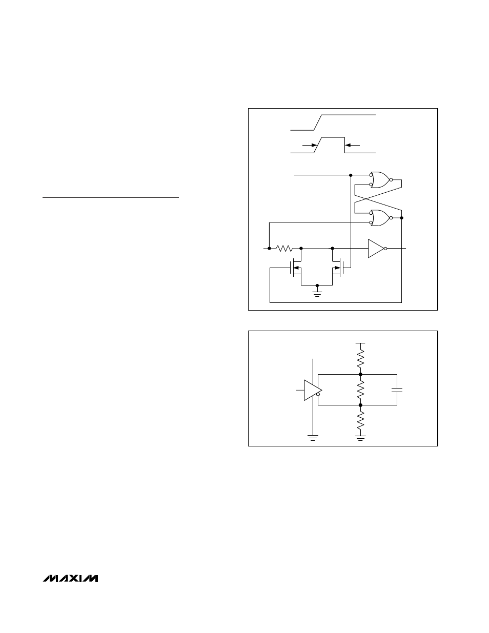
Hot-Swap Input Circuitry
In the MAX3030E–MAX3033E, the enable inputs feature
hot-swap capability. At the input there are two NMOS
devices, M1 and M2 (Figure 10). When V
CC
is ramping
up from zero, an internal 6µs timer turns on M2 and sets
the SR latch, which also turns on M1. Transistors M2, a
2mA current sink, and M1, a 100µA current sink, pull EN
to GND through a 5.6k
Ω resistor. M2 is designed to pull
the EN input to the disabled state against an external
parasitic capacitance of up to 100pF that is trying to
enable the EN input. After 6µs, the timer turns M2 off and
M1 remains on, holding the EN input low against three-
state output leakages that might enable EN. M1 remains
on until an external source overcomes the required input
current. At this time the SR latch resets and M1 turns off.
When M1 turns off, EN reverts to a standard, high-
impedance CMOS input. Whenever V
CC
drops below
1V, the hot-swap input is reset. The EN1&2 and EN3&4
input structures are identical to the EN input. For the EN
input, there is a complementary circuit employing two
PMOS devices pulling the EN input to V
CC
.
Hot-Swap Line Transient
The circuit of Figure 11 shows a typical offset termina-
tion used to guarantee a greater than 200mV offset
when a line is not driven. The 50pF capacitor repre-
MAX3030E–MAX3033E
±15kV ESD-Protected, 3.3V Quad
RS-422 Transmitters
_______________________________________________________________________________________
9
EN
DE
(HOT SWAP)
5.6k
Ω
TIMER
TIMER
V
CC
6
µs
M2
M1
2mA
100
µA
Figure 10. Simplified Structure of the Driver Enable Pin (EN)
V
CC
DI_
(V
CC
OR GND)
3.3V
DO_+
DO_-
50pF
0.1k
Ω
1k
Ω
1k
Ω
Figure 11. Differential Power-Up Glitch (Hot Swap)
