Test circuits and timing diagrams – Rainbow Electronics MAX3033E User Manual
Page 7
MAX3030E–MAX3033E
±15kV ESD-Protected, 3.3V Quad
RS-422 Transmitters
_______________________________________________________________________________________
7
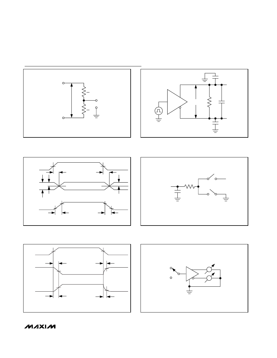
Test Circuits and Timing Diagrams
DI_
V
OD
R
L
C
L
C
L
C
L
DO_+
DO_-
Figure 2. Differential Driver Propagation Delay and Transition
Time Test Circuit
V
OC
V
OD
DI_+
DI_-
R
L
2
R
L
2
Figure 1. Differential Driver DC Test Circuit
OUTPUT
UNDER TEST
C
L
R
L
V
CC
S1
S2
ENABLE SIGNAL IS ONE OF THE POSSIBLE
ENABLE CONFIGURATIONS (SEE TRUTH TABLE).
Figure 4. Driver Enable/Disable Delays Test Circuit
DI
3V
0V
DO_-
DO_+
V
O
0V
-V
O
V
O
1.5V
1.5V
t
DPLH
t
DPHL
1/2 V
O
10%
t
R
90%
90%
1/2 V
O
10%
t
F
V
DIFF
= V (DO_+) - V (DO_-)
V
DIFF
t
SKEW
=
|t
DPLH
-
t
DPHL
|
Figure 3. Differential Driver Propagation Delay and Transition
Waveform
OUTPUT NORMALLY LOW
OUTPUT NORMALLY HIGH
3V
0V
V
OL
0V
1.5V
1.5V
1.5V
1.5V
EN
V
OH
t
DZL
t
DZH
t
DLZ
t
DHZ
V
OL
+ 0.3V
V
OH
- 0.3V
ENABLE SIGNAL IS ONE OF THE POSSIBLE
ENABLE CONFIGURATIONS (SEE TRUTH TABLE).
Figure 5. Driver Enable/Disable Waveform
DI
V
CC
GND
A
A
DO_-
DO_+
Figure 6. Short-Circuit Measurements