Logic electrical characteristics, Lm82 – Rainbow Electronics LM82 User Manual
Page 7
Logic Electrical Characteristics
(Continued)
Note 1: Absolute Maximum Ratings indicate limits beyond which damage to the device may occur. DC and AC electrical specifications do not apply when operating
the device beyond its rated operating conditions.
Note 2: When the input voltage (V
I
) at any pin exceeds the power supplies (V
I
<
GND or V
I
>
V
CC
), the current at that pin should be limited to 5 mA. The 20 mA
maximum package input current rating limits the number of pins that can safely exceed the power supplies with an input current of 5 mA to four.
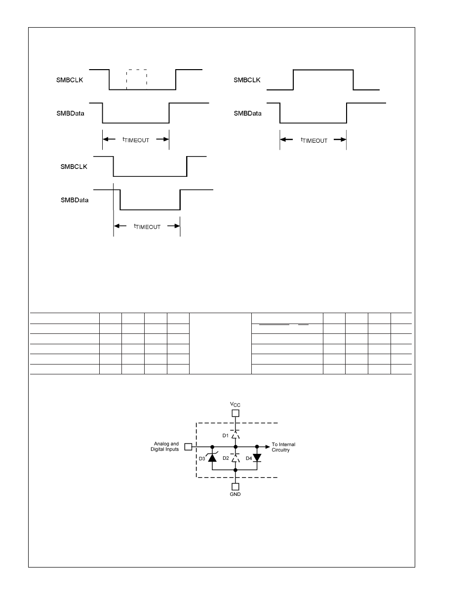
Parasitic components and or ESD protection circuitry are shown in the figure below for the LM82’s pins. The nominal breakdown voltage of the zener D3 is 6.5 V.
Care should be taken not to forward bias the parasitic diode, D1, present on pins: D+, D−, ADD1 and ADD0. Doing so by more than 50 mV may corrupt a temperature
or voltage measurement.
Pin Name
D1
D2
D3
D4
Pin Name
D1
D2
D3
D4
NC (pins 1 & 5)
T_CRIT_A & INT
x
V
CC
x
SMBData
x
x
D+
x
x
x
NC (pins 9 & 15)
x
x
x
D−
x
x
x
x
SMBCLK
x
x
ADD0, ADD1
x
x
x
NC (pin 13)
x
x
Note: An x indicates that the diode exists.
Note 3: See AN-450 “Surface Mounting Methods and Their Effect on Product Reliability” or the section titled “Surface Mount” found in a current National Semicon-
ductor Linear Data Book for other methods of soldering surface mount devices.
Note 4: Human body model, 100 pF discharged through a 1.5 k
Ω
resistor. Machine model, 200 pF discharged directly into each pin.
Note 5: Thermal resistance of the QSOP-16 package is 130˚C/W, junction-to-ambient when attached to a FR-4 printed circuit board with 1 oz. foil as shown in
Fig-
ure 3 .
SMBus TIMEOUT
DS101297-7
See drawing DS10129707
DS101297-13
FIGURE 1. ESD Protection Input Structure
LM82
www.national.com
7