Rainbow Electronics MAX1775 User Manual
Page 2
MAX1775
Dual-Output Step-Down
DC-DC Converter for PDA/Palmtop Computers
2
_______________________________________________________________________________________
ABSOLUTE MAXIMUM RATINGS
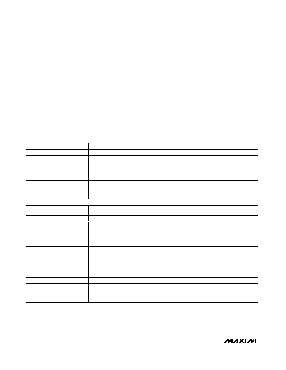
ELECTRICAL CHARACTERISTICS
(V
IN
= +12V, V
MAIN
= V
INC
= V
CS-
= V
CS+
= +3.3V, V
CORE
= +1.8V, Circuit of Figure 4, T
A
= 0°C to +85°C, unless otherwise noted.
Typical values are at T
A
= +25°C.)
Stresses beyond those listed under “Absolute Maximum Ratings” may cause permanent damage to the device. These are stress ratings only, and functional
operation of the device at these or any other conditions beyond those indicated in the operational sections of the specifications is not implied. Exposure to
absolute maximum rating conditions for extended periods may affect device reliability.
IN, SHDNM, CVH to GND.......................................-0.3V to +30V
IN to CVH, PDRV ......................................................-0.3V to +6V
PDRV to GND..................................(V
CVH
- 0.3V) to (V
IN
+ 0.3V)
PGND to GND .......................................................-0.3V to +0.3V
All Other Pins to GND...............................................-0.3V to +6V
Core Output Short Circuit...........................................Continuous
Continuous Power Dissipation
16-Pin QSOP (derate 7.1mW/°C above +70°C)..........571mW
Operating Temperature .......................................-40°C to +85°C
Storage Temperature.........................................-65°C to +150°C
Lead Temperature (soldering, 10s) .................................+300°C
PARAMETER
SYMBOL
CONDITIONS
MIN
TYP
MAX
UNITS
Input Voltage
V
IN
2.7
28
V
Input Quiescent Supply Current
I
IN
V
FBM
= +1.5V, V
FBC
= +1.5V,
V
SHDNM
= V
SHDNC
= +3.3V
15
30
µA
CS- Quiescent Supply Current
I
CS
-
V
FBM
= +1.5V, V
FBC
= +1.5V,
V
SHDNM
= V
SHDNC
= +3.3V
110
220
µA
Core Regulator Quiescent
Supply Current
I
INC
V
FBM
= +1.5V, V
FBC
= +1.5V,
V
SHDNM
= V
SHDNC
= +3.3V
60
120
µA
IN Shutdown Supply Current
SHDNM = SHDNC = GND
5
30
µA
MAIN REGULATOR
Main Output Voltage Adjust
Range
1.25
5.5
V
FBM Regulation Threshold
V
FBM
V
( C S + - C S - )
= 0 to + 60m V , V
IN
= + 2.7V to + 28V 1.21
1.25
1.29
V
FBM Input Current
I
FBM
V
FBM
= +1.3V
-0.1
0.1
µA
Current-Limit Threshold
V
CLM
V
CS+
- V
CS-
60
80
100
mV
Minimum Current-Limit
Threshold
V
MIN
V
CS+
- V
CS
-
6
15
24
mV
Valley Current Threshold
V
VALLEY
V
CS+
- V
CS
-
40
50
60
mV
Zero Current Threshold
V
ZERO
V
CS+
- V
CS
-
0
15
mV
PDRV, NDRV Gate Drive
Resistance
V
CS
- = +3.3V, I
LOAD
= 50mA
2
4.4
Ω
CS- to CVL Switch Resistance
I
CVL
= 50mA
4.5
8
Ω
PDRV, NDRV Dead Time
50
ns
Maximum Duty Cycle
100
%
Minimum On-Time
200
400
650
ns
Minimum Off-Time
200
400
650
ns