Rainbow Electronics MAX1775 User Manual
Page 12
MAX1775
Dual-Output Step-Down
DC-DC Converter for PDA/Palmtop Computers
12
______________________________________________________________________________________
pulses and low efficiency. This feature, however, is dis-
abled during dropout and light-load conditions where
the inductor current may take too long to reach the I
MIN
value. A watchdog timer overrides I
MIN
after the P-
channel MOSFET has been on for longer than about
10µs.
Main Step-Down Converter
The main step-down converter features adjustable
+1.25V to +5.5V output, delivering over 2A from a
+2.7V to +28V input (see Setting the Output Voltages).
The use of external MOSFETs and a current-sense
resistor maximizes design flexibility. The MAX1775
offers a synchronous rectifier MOSFET driver that
improves efficiency by eliminating losses through a
diode. The two MOSFET drive outputs, PDRV and
NDRV, control these external MOSFETs. The output
swing of these outputs is limited to reduce power con-
sumption by limiting the amount of injected gate charge
(see Internal Linear Regulators). The main current limit
is sensed through a small sense resistor at the convert-
er output (see Setting the Current Limit). Driving SHDNM
low puts the main converter in a low-power shutdown
mode. The core regulator is still functional when the
main converter is in shutdown.
Core Step-Down Converter
The core step-down converter produces a +1.0V to
+5.0V output from a +2.6V to +5.5V input. The low-volt-
age input allows the use of internal power MOSFETs, tak-
ing advantage of their low R
DS(ON)
, improving efficiency
and reducing board space. Like the main converter, the
core regulator makes use of an N-channel MOSFET syn-
chronous rectifier, improving efficiency and eliminating
the need for an external Schottky diode. Current sensing
is internal to the device, eliminating the need for an
external sense resistor. The maximum and minimum cur-
rent limits are sensed through the P-channel MOSFET,
while the valley current and zero crossing current are
sensed through the N-channel MOSFET. The core output
voltage is measured at FBC through a resistive voltage-
divider. This divider can be adjusted to set the output
voltage level (see Setting the Output Voltages). The core
input can be supplied from the main regulator or an
external supply that does not exceed +5.5V (see High-
Voltage Configuration and Low-Voltage Configuration).
The core converter can be shut down independent of the
main converter by driving SHDNC low. If the main con-
verter output is supplying power to the core and is shut
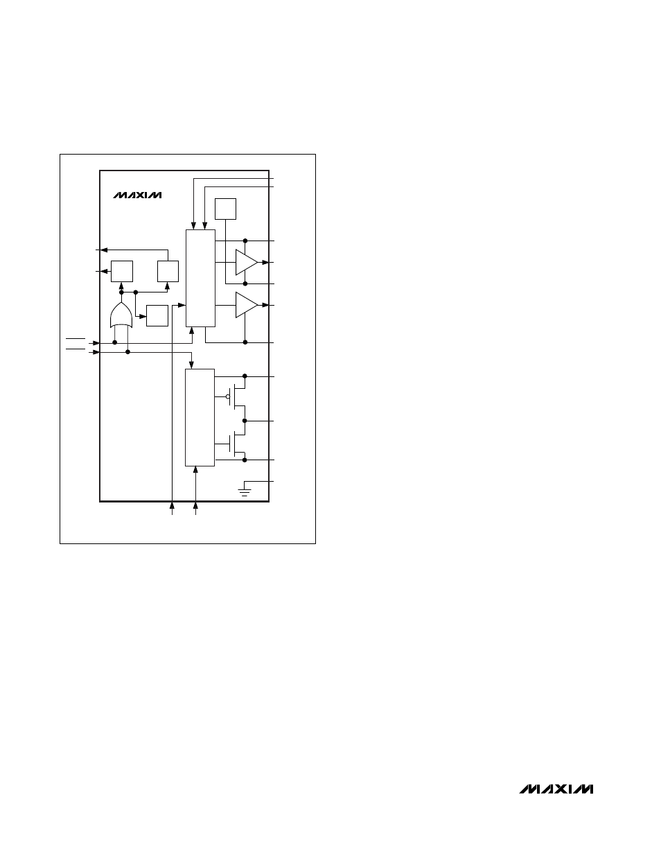
down, SHDNM controls both outputs. Figure 3 is a sim-
plified block diagram.
Internal Linear Regulators
There are two linear regulators internal to the MAX1775. A
high-voltage linear regulator accepts inputs up to +28V,
reducing it to +2.8V at CVL to provide power to the
MAX1775. Once the voltage at CS- reaches +2.47V, CVL
is switched to CS, allowing it to be driven from the main
converter, improving efficiency. CVL supplies the internal
bias to the IC and power for the NDRV gate driver.
The CVH regulator provides the low-side voltage for the
main regulator’s PDRV output. The voltage at CVH is reg-
ulated at 4.3V below V
IN
to limit the voltage swing on
PDRV, reducing gate charge and improving efficiency
(Figure 3).
Reference
The MAX1775 has an accurate internally trimmed
+1.25V reference at REF. REF can source no more than
50µA. Bypass REF to GND with a 0.22µF capacitor.
CVH
IN
CS+
CS-
PDRV
NDRV
PGND
CVH
CVL
SOFT-
START
REF
CVL
REF
SHDNM
SHDNC
CS-
FB
ON
CS+
MAIN
BUCK
MAIN
OUT
INC
LXC
GND
PGNDC
ON
FB
FBM
FBC
CORE
BUCK
MAX1775
Figure 3. Simplified Block Diagram