Detailed description – Rainbow Electronics MAX3295 User Manual
Page 8
MAX3293/MAX3294/MAX3295
20Mbps, +3.3V, SOT23 RS-485/
RS-422 Transmitters
8
_______________________________________________________________________________________
Detailed Description
The MAX3293/MAX3294/MAX3295 are low-power
transmitters for RS-485/RS-422 communication. The
MAX3295 operates at data rates up to 20Mbps, the
MAX3294 up to 2.5Mbps (slew-rate limited), and the
MAX3293 up to 250kbps (slew-rate limited). These
devices are enabled using an active-high driver enable
(DE) input. When disabled, outputs enter a high-imped-
ance state, and the supply current reduces to 1µA.
The MAX3293/MAX3294/MAX3295 have a hot-swap
input structure that prevents disturbance on the differ-
ential signal lines when a circuit board is plugged into
a “hot” backplane (see the Hot-Swap Capability sec-
tion). Drivers are also short-circuit current limited and
are protected against excessive power dissipation by
thermal-shutdown circuitry.
Driver
The driver accepts a single-ended, logic-level input
(DI) and translates it to a differential RS-485/RS-422
level output (Y and Z). Driving DE high enables the dri-
ver, while pulling DE low places the driver outputs
(Y and Z) into a high-impedance state (see Table 1).
Low-Power Shutdown
Force DE low to disable the MAX3293/MAX3294/
MAX3295. In shutdown mode, the device consumes a
maximum of 10µA of supply current.
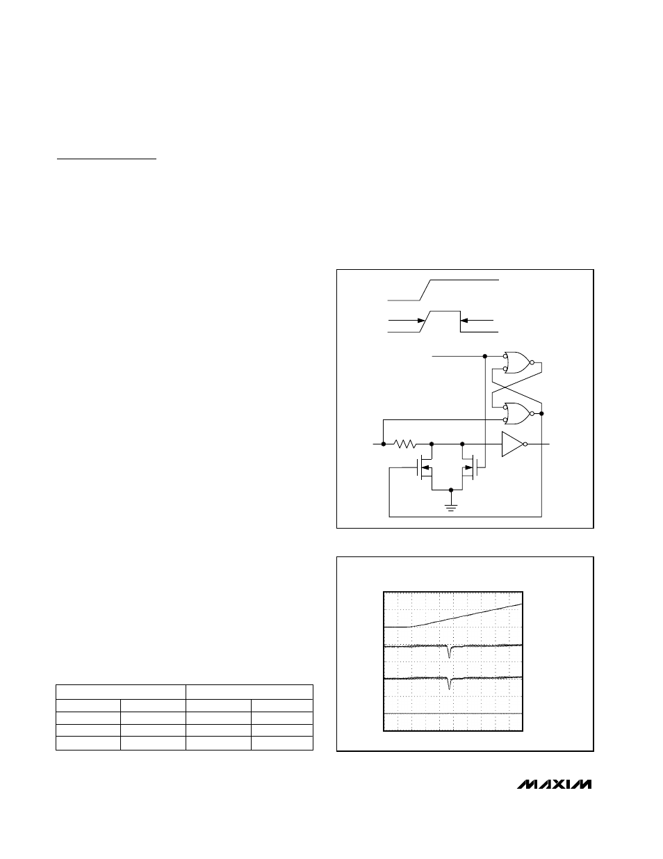
Hot-Swap Capability
Hot-Swap Input
When circuit boards are inserted into a “hot” or pow-
ered backplane, disturbances to the enable can lead to
data errors. Upon initial circuit board insertion, the
processor undergoes its power-up sequence. During
this period, the output drivers are high impedance and
are unable to drive the DE input of the MAX3293/
MAX3294/MAX3295 to a defined logic level. Leakage
currents up to 10µA from the high-impedance output
could cause DE to drift to an incorrect logic state.
Additionally, parasitic circuit board capacitance could
cause coupling of V
CC
or GND to DE. These factors
could improperly enable the driver.
The MAX3293/MAX3294/MAX3295 eliminate all above
issues with hot-swap circuitry. When V
CC
rises, an
internal pulldown circuit holds DE low for approximately
10µs. After the initial power-up sequence, the pulldown
circuit becomes transparent, resetting the hot-swap tol-
erable input.
Table 1. MAX3293/MAX3294/
MAX3295 (RS-485/RS-422) Transmitting
Function Table
X = Don’t care.
INPUTS
OUTPUTS
DE
DI
Y
Z
0
X
Shutdown
Shutdown
1
0
0
1
1
1
1
0
V
CC
TIMER
TIMER
EN
DE
(HOT SWAP)
10
µs
100
µA
M1
M2
5.6k
Ω
2mA
Figure 6. Simplified Structure of the Driver Enable Input (DE)
Figure 7. Differential Power-Up Glitch (0.1V/µs)
DIFFERENTIAL POWER-UP GLITCH
(0.1V/
µs)
4
µs/div
2V/div
V
CC
Y
Z
Y-Z
0V
10mV/div
AC-COUPLED
10mV/div
AC-COUPLED
20mV/div