Pin description detailed description – Rainbow Electronics MAX1618 User Manual
Page 6
MAX1618
Remote Temperature Sensor
with SMBus Serial Interface
6
_______________________________________________________________________________________
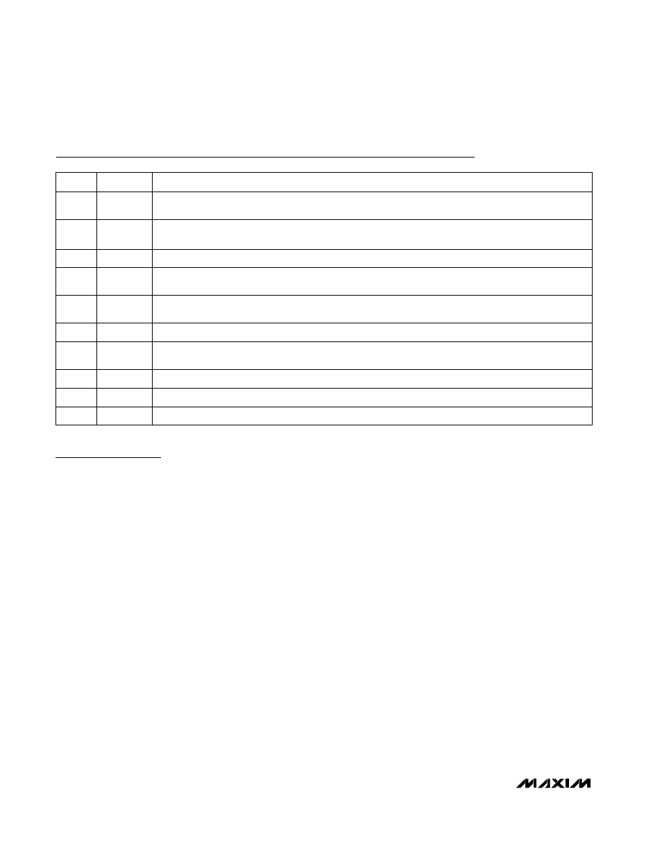
Pin Description
Detailed Description
The MAX1618 is a temperature sensor designed to
work in conjunction with an external microcontroller
(µC) or other intelligence in thermostatic, process-con-
trol, or monitoring applications. The µC is typically a
power-management or keyboard controller, generating
SMBus serial commands by “bit-banging” general-pur-
pose input-output (GPIO) pins or through a dedicated
SMBus interface block.
Essentially an 8-bit serial analog-to-digital converter
(ADC) with a sophisticated front end, the MAX1618
contains a switched-current source, a multiplexer, an
ADC, an SMBus interface, and the associated control
logic (Figure 1). Temperature data from the ADC is
loaded into a data register, where it is automatically
compared with data previously stored in over/under-
temperature alarm threshold registers. The alarm
threshold registers can be set for hysteretic fan control.
ADC and Multiplexer
The averaging ADC integrates over a 30ms period (typ)
with excellent noise rejection. The ADC converts at a
rate of 16Hz. The multiplexer automatically steers bias
currents through the remote diode, measures the for-
ward voltage, and computes the temperature.
The DXN input is biased at 0.65V above ground by an
internal diode to set up the analog-to-digital (A/D)
inputs for a differential measurement. The worst-case
DXP-DXN differential input voltage range is 0.25V to
0.95V.
Excess resistance in series with the remote diode
causes about +1/2°C error/
Ω. A 200µV offset voltage at
DXP-DXN causes about +1°C error.
A/D Conversion Sequence
If a Start command is written (or generated automatical-
ly in the free-running autoconvert mode), the result of
the measurement is available after the end of conver-
sion. A BUSY status bit in the status byte shows that the
device is performing a new conversion. The result of the
previous conversion is always available even when the
ADC is busy.
SMBus Serial-Data Input/Output. Open drain.
SMBDATA
9
SMBus Alert (Interrupt) Output. Open drain.
ALERT
10
Combined Current Source and A/D Positive Input. Do not leave DXP floating. Place a 2200pF capacitor
between DXP and DXN for noise filtering.
DXP
5
Supply Voltage Input. Bypass to GND with a 0.1µF capacitor.
V
CC
6
Hardware-Standby Input. Temperature and comparison threshold data are retained in standby mode.
Low = standby mode. High = operating mode.
STBY
7
SMBus Serial-Clock Input
SMBCLK
8
Combined Current Sink and A/D Negative Input. DXN is normally biased to a diode voltage above
ground.
DXN
4
Ground
GND
3
PIN
SMBus Slave Address Select Input. (See Table 6.) ADD0 and ADD1 are sampled upon power-up. Excess
capacitance (>50pF) at the address pins when floating may cause address-recognition problems.
ADD1
2
SMBus Slave Address Select Input. (See Table 6.) ADD0 and ADD1 are sampled upon power-up. Excess
capacitance (>50pF) at the address pins when floating may cause address-recognition problems.
ADD0
1
FUNCTION
NAME