Design procedure – Rainbow Electronics MAX799 User Manual
Page 19
MAX796/MAX797/MAX799
Step-Down Controllers with
Synchronous Rectifier for CPU Power
______________________________________________________________________________________
19
_________________Design Procedure
The five pre-designed standard application circuits
(Figure 1 and Table 1) contain ready-to-use solutions
for common applications. Use the following design pro-
cedure to optimize the basic schematic for different
voltage or current requirements. Before beginning a
design, firmly establish the following:
V
IN(MAX)
, the maximum input (battery) voltage.
This
value should include the worst-case conditions, such
as no-load operation when a battery charger or AC
adapter is connected but no battery is installed.
V
IN(MAX)
must not exceed 30V. This 30V upper limit is
determined by the breakdown voltage of the BST float-
ing gate driver to GND (36V absolute maximum).
V
IN(MIN)
, the minimum input (battery) voltage.
This
should be taken at full-load under the lowest battery
conditions. If V
IN(MIN)
is less than 4.5V, a special circuit
must be used to externally hold up VL above 4.8V. If
the minimum input-output difference is less than 1.5V,
the filter capacitance required to maintain good AC
load regulation increases.
Inductor Value
The exact inductor value isn’t critical and can be
adjusted freely in order to make tradeoffs among size,
cost, and efficiency. Although lower inductor values will
minimize size and cost, they will also reduce efficiency
due to higher peak currents. To permit use of the physi-
cally smallest inductor, lower the inductance until the
circuit is operating at the border between continuous
and discontinuous modes. Reducing the inductor value
even further, below this crossover point, results in dis-
continuous-conduction operation even at full load. This
helps reduce output filter capacitance requirements but
causes the core energy storage requirements to
increase again. On the other hand, higher inductor val-
ues will increase efficiency, but at some point resistive
losses due to extra turns of wire will exceed the benefit
gained from lower AC current levels. Also, high induc-
tor values can affect load-transient response; see the
V
SAG
equation in the
Low-Voltage Operation
section.
The following equations are given for continuous-con-
duction operation since the MAX796 is mainly intended
for high-efficiency battery-powered applications. See
Appendix A in Maxim’s
Battery Management and DC-
DC Converter Circuit Collection
for crossover point and
discontinuous-mode equations. Discontinuous conduc-
tion doesn’t affect normal idle-mode operation.
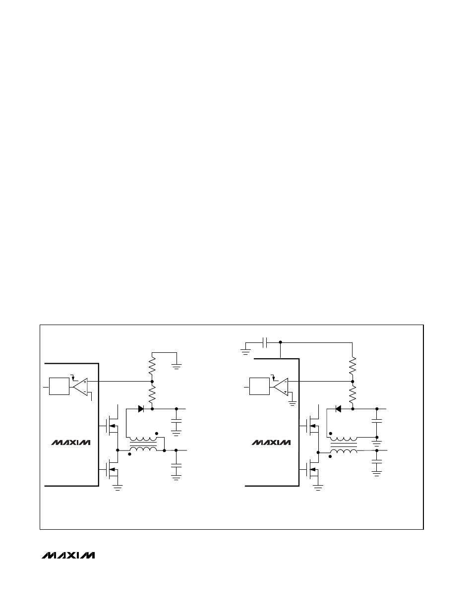
MAX799
NEGATIVE
SECONDARY
OUTPUT
MAIN
OUTPUT
DH
V+
SECFB
R3
R2
1-SHOT
TRIG
DL
0.33
µ
F
REF
MAX796
POSITIVE
SECONDARY
OUTPUT
MAIN
OUTPUT
DH
V+
SECFB
2.505V REF
R3
R2
1-SHOT
TRIG
DL
+V
TRIP
WHERE V
REF
(NOMINAL) = 2.505V
= V
REF
(
1 + –––
)
R2
R3
-V
TRIP
R3 = 100k
Ω
(RECOMMENDED)
= -V
REF
(
–––
)
R2
R3
Figure 9. Secondary-Output Feedback Dividers, MAX796 vs. MAX799