Rainbow Electronics MAX799 User Manual
Page 16
MAX796/MAX797/MAX799
Step-Down Controllers with
Synchronous Rectifier for CPU Power
16
______________________________________________________________________________________
It’s often possible to achieve a bootstrap-like effect, even
for circuits that are set to V
OUT
< 4.5V, by powering VL
from an external-system +5V supply. To achieve this
pseudo-bootstrap, add a Schottky diode between the
external +5V source and VL, with the cathode to the VL
side. This circuit provides a 1% to 2% efficiency boost
and also extends the minimum battery input to less than
4V. The external source must be in the range of 4.8V to
6V. Another way to achieve a pseudo-bootstrap is to add
an extra flyback winding to the main inductor to generate
the +5V bootstrap source, as shown in the +3.3V/+5V
Dual-Output Application (Figure 12).
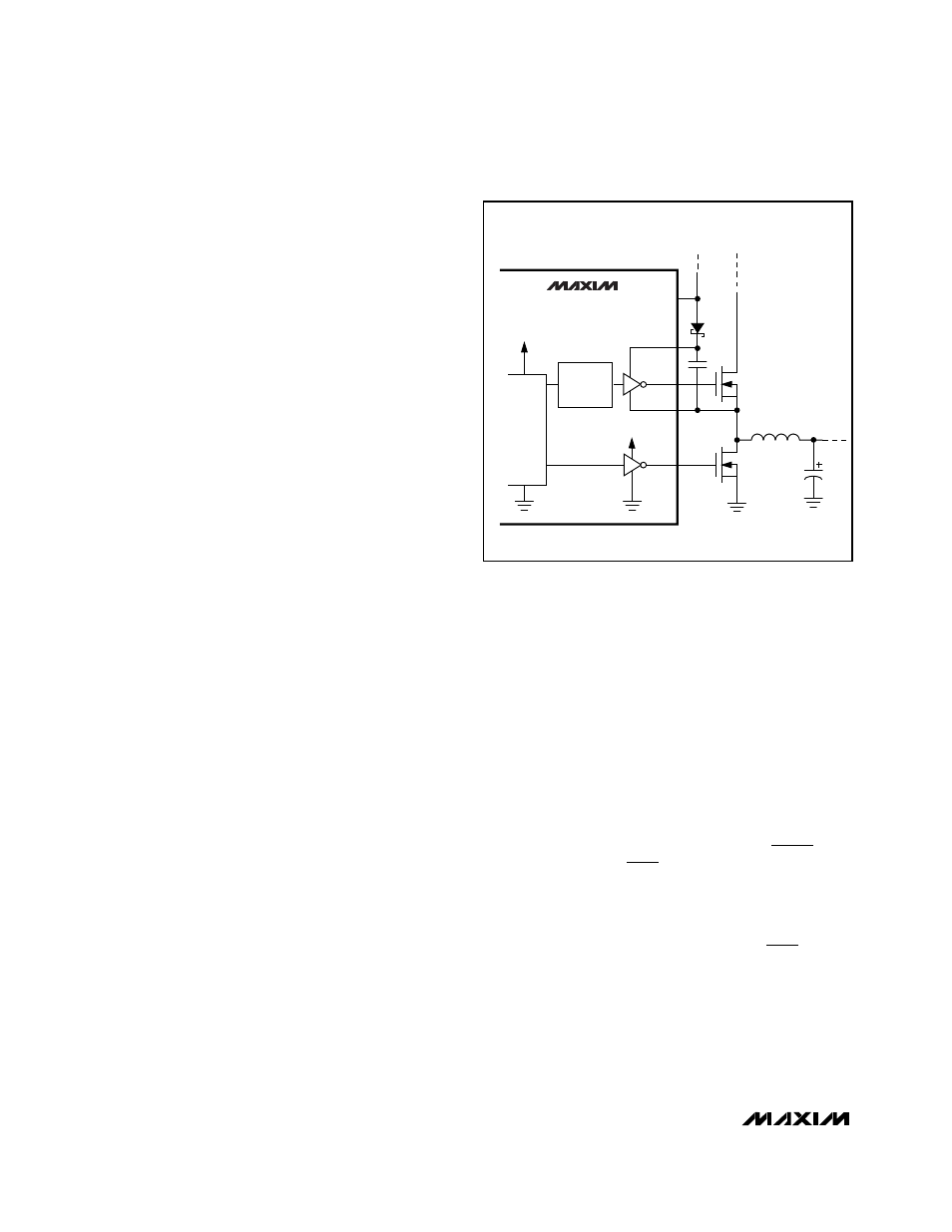
Boost High-Side
Gate-Driver Supply (BST Pin)
Gate-drive voltage for the high-side N-channel switch is
generated by a flying-capacitor boost circuit as shown
in Figure 5. The capacitor is alternately charged from
the VL supply and placed in parallel with the high-side
MOSFET’s gate-source terminals.
On start-up, the synchronous rectifier (low-side MOS-
FET) forces LX to 0V and charges the BST capacitor to
5V. On the second half-cycle, the PWM turns on the
high-side MOSFET by closing an internal switch
between BST and DH. This provides the necessary
enhancement voltage to turn on the high-side switch,
an action that “boosts” the 5V gate-drive signal above
the battery voltage.
Ringing seen at the high-side MOSFET gate (DH) in
discontinuous-conduction mode (light loads) is a natur-
al operating condition, and is caused by the residual
energy in the tank circuit formed by the inductor and
stray capacitance at the switching node LX. The gate-
driver negative rail is referred to LX, so any ringing
there is directly coupled to the gate-drive output.
Current-Limiting and
Current-Sense Inputs (CSH and CSL)
The current-limit circuit resets the main PWM latch and
turns off the high-side MOSFET switch whenever the
voltage difference between CSH and CSL exceeds
100mV. This limiting is effective for both current flow
directions, putting the threshold limit at ±100mV. The
tolerance on the positive current limit is ±20%, so the
external low-value sense resistor must be sized for
80mV/R1 to guarantee enough load capability, while
components must be designed to withstand continuous
current stresses of 120mV/R1.
For breadboarding purposes or very high-current appli-
cations, it may be useful to wire the current-sense inputs
with a twisted pair rather than PC traces. This twisted
pair needn’t be anything special, perhaps two pieces of
wire-wrap wire twisted together.
Oscillator Frequency and
Synchronization (SYNC Pin)
The SYNC input controls the oscillator frequency.
Connecting SYNC to GND or to VL selects 150kHz
operation; connecting SYNC to REF selects 300kHz.
SYNC can also be used to synchronize with an external
5V CMOS or TTL clock generator. SYNC has a guaran-
teed 190kHz to 340kHz capture range.
300kHz operation optimizes the application circuit for
component size and cost. 150kHz operation provides
increased efficiency and improved load-transient
response at low input-output voltage differences (see
Low-Voltage Operation
section).
Low-Noise Mode (SKIP Pin)
The low-noise mode (SKIP = high) is useful for minimiz-
ing RF and audio interference in noise-sensitive appli-
cations such as Soundblaster™ hi-fi audio-equipped
systems, cellular phones, RF communicating comput-
ers, and electromagnetic pen-entry systems. See the
summary of operating modes in Table 3. SKIP can be
driven from an external logic signal.
The MAX797 can reduce interference due to switching
noise by ensuring a constant switching frequency
regardless of load and line conditions, thus concentrat-
ing the emissions at a known frequency outside the
system audio or IF bands. Choose an oscillator fre-
MAX796
MAX797
MAX799
BST
VL
+5V
VL SUPPLY
BATTERY
INPUT
VL
VL
DH
LX
DL
PWM
LEVEL
TRANSLATOR
Figure 5. Boost Supply for Gate Drivers
Soundblaster is a trademark of Creative Labs.