Standard application circuit, Detailed description – Rainbow Electronics MAX799 User Manual
Page 10
MAX796/MAX797/MAX799
Step-Down Controllers with
Synchronous Rectifier for CPU Power
10
______________________________________________________________________________________
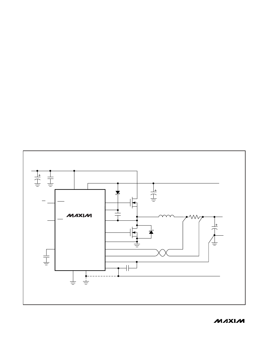
______Standard Application Circuit
It is easy to adapt the basic MAX797 single-output 3.3V
buck converter (Figure 1) to meet a wide range of
applications with inputs up to 28V (limited by choice of
external MOSFET). Simply substitute the appropriate
components from Table 1. These circuits represent a
good set of tradeoffs between cost, size, and efficiency
while staying within the worst-case specification limits
for stress-related parameters such as capacitor ripple
current. Each of these circuits is rated for a continuous
load current at T
A
= +85°C, as shown. The 1A, 2A and
10A applications can withstand a continuous output
short-circuit to ground. The 3A and 5A applications can
withstand a short circuit of many seconds duration, but
the synchronous-rectifier MOSFET overheats, exceed-
ing the manufacturer’s ratings for junction temperature
by 50°C or more.
If the 3A or 5A circuit must be guaranteed to withstand
a continuous output short circuit indefinitely, see the
section
MOSFET Switches
under
Selecting Other
Components
. Don’t change the frequency of these cir-
cuits without first recalculating component values (par-
ticularly inductance value at maximum battery voltage).
_______________Detailed Description
The MAX796 is a BiCMOS, switch-mode power-supply
controller designed primarily for buck-topology regula-
tors in battery-powered applications where high effi-
ciency and low quiescent supply current are critical.
The MAX796 also works well in other topologies such
as boost, inverting, and CLK due to the flexibility of its
floating high-speed gate driver. Light-load efficiency is
enhanced by automatic idle-mode operation—a vari-
able-frequency pulse-skipping mode that reduces
MAX797
CSL
CSH
VL
SYNC
FB
V+
10
11
5
7
14
Q1
Q2
16
15
13
D2
CMPSH-3
J1
150kHz/300kHz
JUMPER
NOTE: KEEP CURRENT-SENSE
LINES SHORT AND CLOSE
TOGETHER. SEE FIG. 10
D1
12
8
9
REF
3
GND
4
+5V AT
5mA
+3.3V
OUTPUT
GND
OUT
BST
DH
LX
DL
2
1
LOW-NOISE
CONTROL
PGND
SKIP
SS
6
ON/OFF
CONTROL
SHDN
INPUT
REF OUTPUT
+2.505V AT 100
µ
A
C5
0.33
µ
F
C4
4.7
µ
F
C7
0.1
µ
F
C6
0.01
µ
F
(OPTIONAL)
C1
C2
C3
0.1
µ
F
R1
L1
Figure 1. Standard 3.3V Application Circuit