Figure 1. esd protection input structure, Note 1), Note 2) – Rainbow Electronics LM95221 User Manual
Page 6: Note 3), Note 4), Note 6), Note 7), Note 8), Note 9), Note 11)
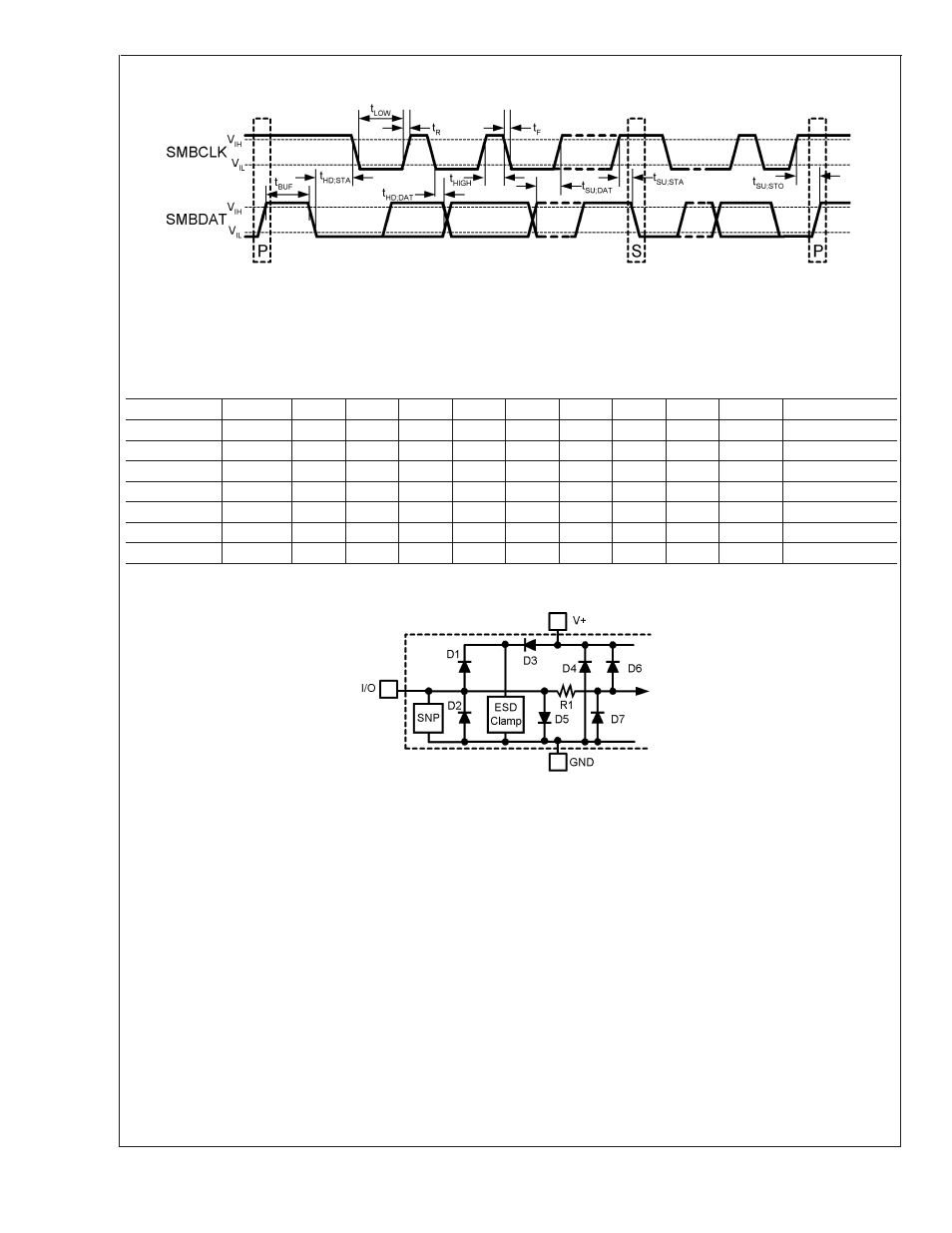
SMBus Communication
20094309
Note 1: Absolute Maximum Ratings indicate limits beyond which damage to the device may occur. DC and AC electrical specifications do not apply when operating
the device beyond its rated operating conditions.
Note 2: When the input voltage (V
I
) at any pin exceeds the power supplies (V
I
<
GND or V
I
>
V
DD
), the current at that pin should be limited to 5 mA.
Parasitic components and or ESD protection circuitry are shown in the figure below for the LM95221’s pins. The nominal breakdown voltage of D4 is 6.5 V. Care
should be taken not to forward bias the parasitic diode, D1, present on pins: D1+, D2+, D1−, D2−. Doing so by more than 50 mV may corrupt the temperature
measurements.
Pin Name
PIN #
D1
D2
D3
D4
D5
D6
D7
R1
SNP
ESD CLAMP
V
DD
1
x
x
D1+
2
x
x
x
x
x
x
x
D1−
3
x
x
x
x
x
x
x
x
D2+
4
x
x
x
x
x
x
x
D2-
6
x
x
x
x
x
x
x
x
SMBDAT
7
x
x
x
x
x
SMBCLK
8
x
x
x
Note: An “x” indicates that the component exists for the designated pin. SNP refers to a snap-back device.
Note 3: See the URL ”http://www.national.com/packaging/“ for other recommendations and methods of soldering surface mount devices.
Note 4: Human body model, 100pF discharged through a 1.5k
Ω resistor. Machine model, 200pF discharged directly into each pin.
Note 5: Thermal resistance junction-to-ambient when attached to a printed circuit board with 2 oz. foil:
– MSOP-8 = 210˚C/W
Note 6: Typicals are at T
A
= 25˚C and represent most likely parametric norm.
Note 7: Limits are guaranteed to National’s AOQL (Average Outgoing Quality Level).
Note 8: Local temperature accuracy does not include the effects of self-heating. The rise in temperature due to self-heating is the product of the internal power
dissipation of the LM95221 and the thermal resistance. See (Note 5) for the thermal resistance to be used in the self-heating calculation.
Note 9: The accuracy of the LM95221CIMM is guaranteed when using the thermal diode with a non-ideality of 1.008 and series R= 2.7
Ω. When using an
MMBT3904 type transistor as the thermal diode the error band will be offset by -3.25˚C
Note 10: Quiescent current will not increase substantially with an SMBus.
Note 11: This specification is provided only to indicate how often temperature data is updated. The LM95221 can be read at any time without regard to conversion
state (and will yield last conversion result).
Note 12: The output rise time is measured from (V
IN(0)
max + 0.15V) to (V
IN(1)
min − 0.15V).
Note 13: The output fall time is measured from (V
IN(1)
min - 0.15V) to (V
IN(1)
min + 0.15V).
Note 14: Holding the SMBDAT and/or SMBCLK lines Low for a time interval greater than t
TIMEOUT
will reset the LM95221’s SMBus state machine, therefore setting
SMBDAT and SMBCLK pins to a high impedance state.
20094313
FIGURE 1. ESD Protection Input Structure
LM95221
www.national.com
6