Rainbow Electronics MAX1688 User Manual
Page 9
MAX1687/MAX1688
Step-Up DC-DC Converters with
Precise, Adaptive Current Limit for GSM
_______________________________________________________________________________________
9
To set the current limit, apply a voltage of 0 to 1V at
LIM. The current limit is 200mA when V
LIM
= 0 to
0.25V. Use the following equation to calculate I
LIM
:
I
LIM
= V
LIM
(0.86A/V) – 0.06A
where V
LIM
= 0.25V to 1V.
V
LIM
is internally clamped to 1.25V when the voltage
applied at V
LIM
is above 1.25V. Generate V
LIM
by one
of three methods: an externally applied voltage, the
output of a DAC, or a resistor-divider using V
REF
as the
supply voltage (TSSOP packages) (Figure 5). Note that
REF can supply up to 10µA.
Determine V
LIM
as follows:
V
LIM
= (I
LX(PEAK)
+ 0.06A) / 0.86
where I
LX(PEAK)
= [(I
LOAD
·
V
OUT
) / V
IN
] + 0.1A (see
the Inductor Current parameter in the
Typical Operating
Characteristics
).
Setting Recharge Time (MAX1688)
The MAX1688 has a recharging feature employing a
sample-and-hold, which sets the maximum time to
recharge the reservoir capacitor. Synchronize the ON
pin to place the converter in standby during each load
current burst. At the end of each load current burst, the
output voltage is sampled by the MAX1688. This volt-
age controls the peak inductor current. The greater the
difference between the regulated output voltage and
the valley of the sag voltage, the higher the peak cur-
rent. This results in a constant recharge time that com-
pensates for varying output filter capacitor character-
istics as well as a varying input voltage. Therefore, the
circuit demands only as much peak current from the
battery as output conditions require, minimizing the
peak current from the battery. An external resistor
between CHG and GND controls the output recharge
time. A large resistor increases peak inductor current
which speeds up recovery time. Calculate the resistor
as follows:
where:
R
CHG
is the external resistor
I
BURST
is the peak burst current expected
D
GSM
is the duty cycle of GSM
V
IN
is the input voltage
V
OUT
is the output voltage
V
REF
= 1.25V
V
DROOP
is the drop in output voltage during the cur-
rent burst
g
mCHG
is the internal transconductance = 0.8A/V
g
mFB
is the feedback transconductance = 200µA/V
tol is the tolerance of the R
CHG
resistor
For example, for I
BURST
= 2.66A, V
DROOP
= 0.36V, V
IN
= +2.7V, and V
OUT
= 3.6V, then R
CHG
= 31.5k
Ω
, using
a 5% tolerance resistor.
The recovery time for a 40.2k
Ω
R
CHG
is shorter than
that with an 18k
Ω
R
CHG
, but the peak battery current is
higher. See Switching Waveforms (GSM Pulsed Load
1A, R
CHG
= 40.2k
Ω
) and Switching Waveforms (GSM
Pulsed Load 1A, R
CH
= 18k
Ω
) in
Typical Operating
Characteristics
.
Inductor Selection
The value of the inductor determines the switching fre-
quency. Calculate the switching frequency as:
f = V
IN
[1 - (V
IN
/ V
OUT
)] / (L
·
I
RIPPLE
)
where f is the switching frequency, V
IN
is the input volt-
age, V
OUT
is the output voltage, L is the inductor value,
and I
RIPPLE
is the ripple current expected, typically
0.2A. Using a lower value inductor increases the fre-
quency and reduces the physical size of the inductor.
A typical frequency is from 150kHz to 1MHz (see
Switching Frequency vs. Inductance in the
Typical
Operating Characteristics
).
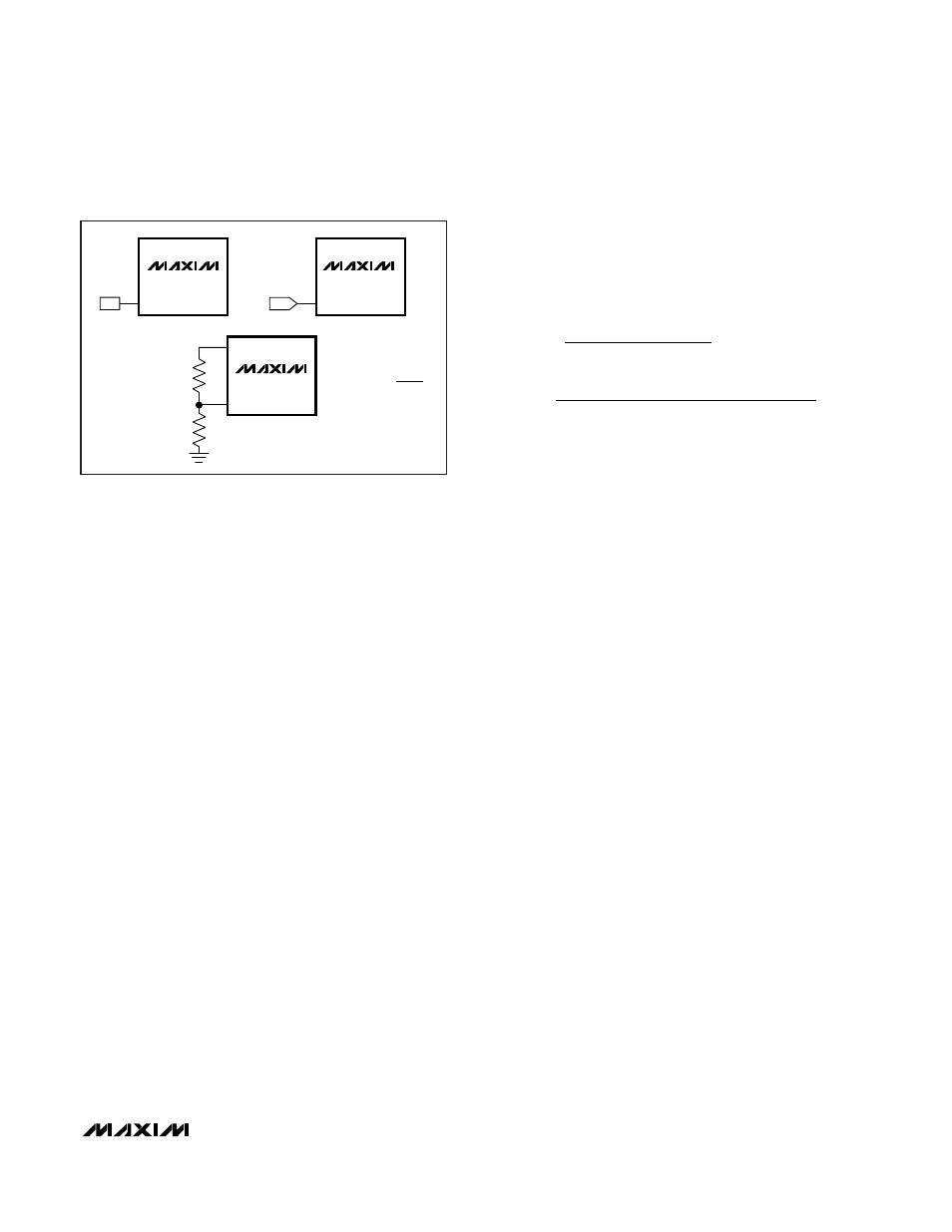
DAC
REF
REF
a)
c)
b)
LIM
LIM
V
LIM(CHG)
= V
REF
R3
+
R4
> 125k
Ω
R4
R4 + R3
R3
R4
LIM
MAX1687
MAX1687
MAX1687
Figure 5. Current-Limit Adjust
R
=
I
V
D
V
1 - D
+ 0.1
V
V
gm
V
gm
1 - tol
CHG
BURST
OUT
GSM
IN(MIN)
GSM
IN(MIN)
DROOP
CHG
REF
FB
⋅
⋅
⋅
⋅
⋅
⋅
⋅
⋅
(
)
(
)
( )