Detailed description, Pin description – Rainbow Electronics MAX1688 User Manual
Page 6
MAX1687/MAX1688
Detailed Description
The MAX1687 and MAX1688 ICs supply power ampli-
fiers in GSM applications where limited input current
surge is desirable. For example, GSM systems require
high-power, 12% duty-cycle RF bursts. Synchronizing
the MAX1687/MAX1688 to enter standby mode during
these RF bursts eliminates battery surge current and
minimizes switching noise to the power amplifier. In
standby mode, the charged output reservoir capacitor
delivers power to the power amplifier. Between each
burst, the DC-DC converter switches on to charge the
output capacitor. To improve efficiency and reduce peak
battery current, the MAX1687/MAX1688 provide a volt-
age-controlled current limit. The MAX1688 is a MAX1687
with added self-regulating circuitry that recharges the
reservoir capacitor in a fixed time (Figure 1).
Start-Up Sequence
In a conventional DC-DC converter, when high current
is required by the load, the battery voltage droops due
to battery series resistance. This may cause other cir-
cuitry that depends on the battery to malfunction or be
reset. The MAX1687/MAX1688 prevent battery voltage
droop by charging the reservoir capacitor during sys-
tem off-time and isolate the battery from the output dur-
ing high current demand. The MAX1687/MAX1688 are
gentle to the battery during initial power-up, as well.
Step-Up DC-DC Converters with
Precise, Adaptive Current Limit for GSM
6
_______________________________________________________________________________________
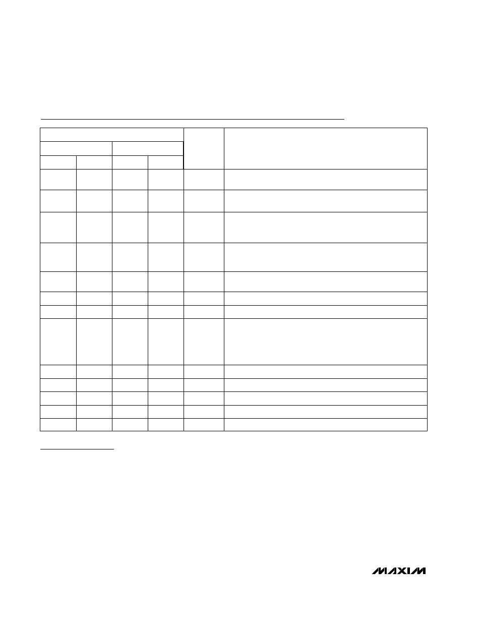
Pin Description
PIN
NAME
FUNCTION
MAX1688
MAX1687
—
10
11, 12
13, 14
15, 16
6
7
8
9
5
—
3, 4
1, 2
TSSOP
GND
AGND
PGND
LX2
OUT
FB
REF
N.C.
ON
CHG
LIM
LX1
IN
Ground
Analog Ground
Power Ground
N-Channel and P-Channel MOSFET Drain
Output
Feedback Input. Connect a resistor-divider from OUT to GND to
set the output voltage. FB regulates to a nominal 1.25V.
Reference Voltage Output. 1.25V nominal.
No Connection. Not internally connected.
Logic ON/OFF Input. When ON is high, the device operates in
normal mode. When ON goes low, the device goes into standby
mode. If ON remains low for greater than 1.2ms, the device shuts
down (see
Standby/Shutdown
section). The supply current falls to
3µA in shutdown mode.
Constant-Recharge-Time Input. Set the recharge time of the out-
put reservoir capacitor by connecting a resistor from CHG to GND
(see
Applications Information
section).
Voltage-Controlled Current-Limit Adjust Input. Apply a voltage
between 0 and 1V to vary the current limit. LIM is internally
clamped to 1.25V.
Internal Current-Sense Resistor Output. Connect the inductor
between LX1 and LX2.
Supply Voltage Input. Connect Battery to IN. Bypass to GND with
a 47µF minimum capacitor.
6
—
6
—
10
—
—
11, 12
—
7
13, 14
7
8
15, 16
8
4
6
4
—
7
—
—
8
—
5
9
5
3
—
—
—
5
3
SO
2
3, 4
2
1
1, 2
1
SO
TSSOP