Rainbow Electronics MAX1688 User Manual
Page 2
MAX1687/MAX1688
Step-Up DC-DC Converters with
Precise, Adaptive Current Limit for GSM
2
_______________________________________________________________________________________
ABSOLUTE MAXIMUM RATINGS
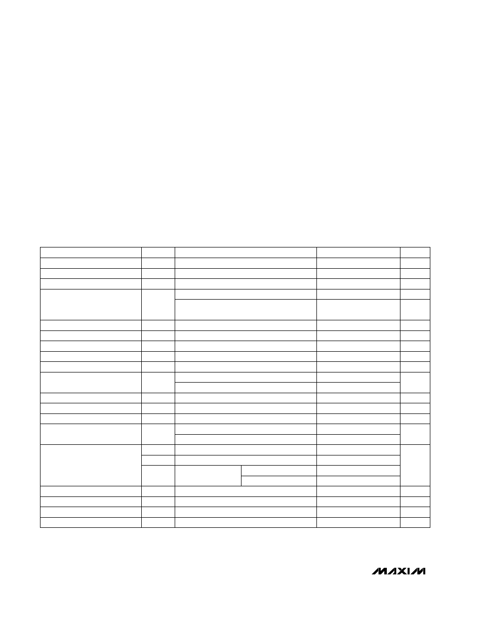
ELECTRICAL CHARACTERISTICS
(V
IN
= V
ON
= +3V, V
LIM
= 1V (MAX1687), V
CHG
= 1V (MAX1688), V
FB
= 1.5V, V
OUT
= 6V,
T
A
= 0°C to +85°C
, unless otherwise noted.
Typical values are at T
A
= +25°C.)
Stresses beyond those listed under “Absolute Maximum Ratings” may cause permanent damage to the device. These are stress ratings only, and functional
operation of the device at these or any other conditions beyond those indicated in the operational sections of the specifications is not implied. Exposure to
absolute maximum rating conditions for extended periods may affect device reliability.
IN, ON, LX1, CHG, LIM, FB, OUT, REF to GND .......-0.3V to +7V
LX2 to GND ..............................................................-0.3V to +8V
IN, LX1 Average Current..........................................................1A
Continuous Power Dissipation (T
A
= +70°C)
TSSOP (derate 5.7mW/°C above +70°C) ....................457mW
SO (derate 5.88mW/°C above +70°C) .........................471mW
Operating Temperature Range ...........................-40°C to +85°C
Storage Temperature Range .............................-65°C to +150°C
Lead Temperature (soldering, 10sec) ............................+300° C
IN rising, 1% hysteresis
V
FB
= 0, V
OUT
= 3V (MAX1688)
V
FB
= 1.125V, V
OUT
= 3V (MAX1688)
V
FB
rising, 2% hysteresis
I
REF
= 0 to 10µA
V
FB
= 1.5V
Shutdown, V
IN
= 4.2V, LX2 connected to LX1,
V
OUT
= 0, ON = GND
V
LIM
= V
CHG
= 1V
CONDITIONS
0.744
0.8
0.856
Peak Current
V
V
REF
6
Output Voltage Range
V
2.4
2.5
2.6
V
2.7
6
Input Voltage Range
Input Undervoltage Lockout
µA
60
110
I
CHG
Source Current
mmho
0.18
0.2
0.22
g
mFB
FB Transconductance
V
1.212
1.250
1.288
FB Set Voltage
V
1.225
1.25
1.275
V
REF
Reference Voltage
mA
2
4
Input Supply Current
µA
3
10
UNITS
MIN
TYP
MAX
SYMBOL
PARAMETER
V
LIM
= V
CHG
= 1V
V
LIM
= V
CHG
= 0.65V
V
IN
= 2.7V
V
LIM
= 1V
V
ON
= 0 or 3V
V
IN
= 2.7V
V
IN
= 6V
V
IN
= 4.2V
V
FB
= 1.5V
V
IN
= 2.7V
Ω
0.3
0.7
P-Channel On-Resistance
Ω
0.1
0.18
R
SENSE
Sense Resistor
mA
170
200
230
I
RIPPLE
A
0.46
0.5
0.54
I
PEAK
Ripple Current
Ω
0.4
0.8
N-Channel On-Resistance
2
0.02
0.1
I
LIM
0.02
0.1
I
ON
V
0.6
V
IL
V
1.8
ON Input Low Voltage
1.5
0.05
0.2
I
FB
Input Current
V
IN
= V
LX2
= 6V, V
OUT
= V
ON
= 0
V
IN
= 4V, V
FB
= 0, V
OUT
= 0
µA
0.05
10
Ω
30
70
Precharge On-Resistance
LX2 Leakage Current
ms
0.7
1.2
1.8
t
DELAY
Shutdown Delay
V
IH
ON Input High Voltage
µA
T
A
= 0°C to +85°C
T
A
= +25°C