Rainbow Electronics MAX1688 User Manual
Page 10
MAX1687/MAX1688
Step-Up DC-DC Converters with
Precise, Adaptive Current Limit for GSM
10
______________________________________________________________________________________
Output (Reservoir) Capacitor
The value of the output capacitor determines the
amount of power available to deliver to the power
amplifier during the RF burst. A larger output capacitor
with low ESR reduces the amount of output voltage
droop during an RF burst. Use the following equation to
determine capacitor size when ON is synchronized to
the RF burst:
where C
OUT
is the output capacitor, I
BURST
is the peak
power amplifier burst current, t
GSM
is the current pulse
period, D
GSM
is the duty cycle, tol is the capacitor tol-
erance, and V
DROOP
is the acceptable drop in the out-
put during the current burst.
For example, when used in a typical GSM system,
t
GSM
= 4.62ms, I
BURST
= 2.66A for a +3.6V system
(1.42A for a +5.5V system), and with a droop of less
than 10%, the value of the capacitor is 5.3mF ±20%.
The output capacitor also determines the constant-load
(ON connected to V
CC
) ripple voltage. The output rip-
ple is:
V
RIPPLE
= I
RIPPLE
·
ESR
(OUTPUT CAPACITOR)
where I
RIPPLE
is typically 0.2A.
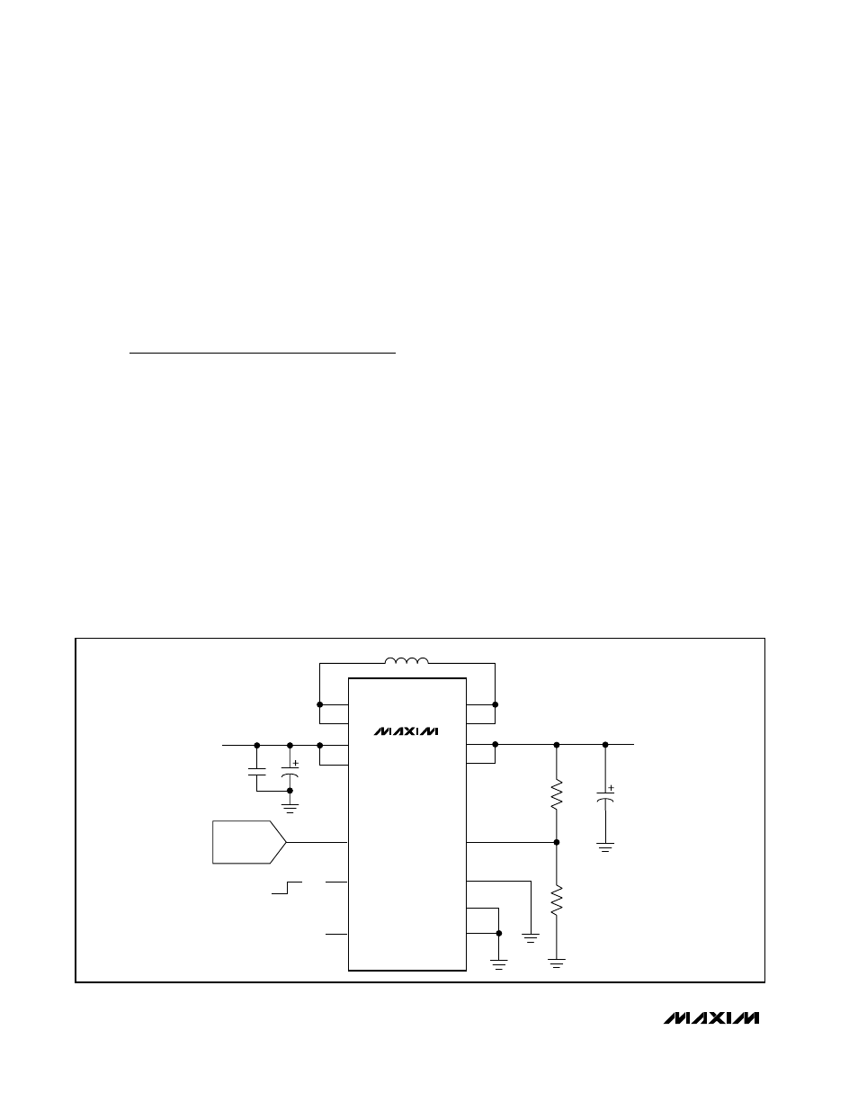
Typical Application Circuits
The current limit of the MAX1687 can be set by an exter-
nal DAC (Figure 6a), making it variable by using a micro-
controller. The MAX1687 is the choice for systems
interfacing with a microcontroller, but may also be used
with fixed current limit (Figure 6b). The MAX1688 can
monitor the droop of the output voltage to set the current
limit, maximizing battery life. The MAX1688 is suitable for
systems demanding variable burst currents (Figures 6a,
6b, and 7) as well as variable input voltages.
Layout
The MAX1687/MAX1688’s high-frequency operation
and high peak currents make PC board layout critical
to minimize ground bounce and noise. Locate input
bypass and output filter capacitors as close to the
device pins as possible. All connections to OUT and FB
should also be kept as short as possible. Use a low-
inductance ground plane. Connect the ground leads of
the input capacitor, output capacitor, and PGND pins in
a star configuration to the ground plane. Table 1 lists
suggested suppliers. Refer to the MAX1687/MAX1688
evaluation kit manual for a suggested surface-mount
layout and a list of suggested components.
C
=
D
I
t
V
- I
ESR
1 - tol
OUT
GSM
BURST
GSM
DROOP
BURST
OUTPUT CAPACITOR
⋅
⋅
⋅
(
)( )
V
OUT
= 5V
2A AT 12%
DUTY CYCLE
OUT
OUT
IN
IN
0.1
µ
F
47
µ
F
V
IN
2.7V TO 6V
10
µ
H
2000
µ
F
R2
187k
R1
61.9k
LX1
LX1
LX2
LX2
ON
ON
OFF
DAC
OUTPUT
0 TO 1V
LIM
REF
FB
AGND
PGND
PGND
MAX1687
Figure 6a. MAX1687 Typical Application Circuit (GSM Pulsed Load)