Applications information – Rainbow Electronics MAX1688 User Manual
Page 8
MAX1687/MAX1688
Step-Up DC-DC Converters with
Precise, Adaptive Current Limit for GSM
8
_______________________________________________________________________________________
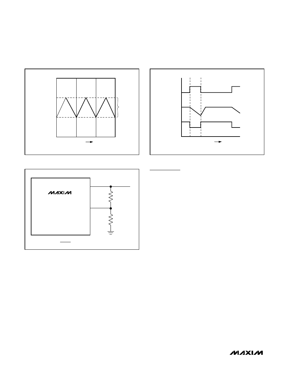
Synchronized ON Pin
If desired, drive ON low during periods of high current
demand to eliminate switching noise from affecting
sensitive RF circuitry. During the periods when ON is
low, the output reservoir capacitor provides current to
the load (Figure 4).
Buck Capability
Although the IC is not intended for this application, the
MAX1687/MAX1688 operate as a buck converter when
the input voltage is higher than the output voltage. The
MAX1687/MAX1688 are not optimally efficient in this
mode (see
Typical Operating Characteristics
for
efficiencies at 2.7V, 3.3V, 5V, and 6V input supply volt-
ages).
Applications Information
Adjusting the Output Voltage
Adjust the MAX1687/MAX1688 output voltage with two
external resistors (Figure 3). Choose R2 to be between
10k
Ω
to 100k
Ω
. Calculate R1 as follows:
R1 = R2
·
(V
OUT
- V
FB
) / V
FB
where V
FB
is the feedback threshold voltage, 1.25V
nominal.
Adjusting Current Limit (MAX1687)
The MAX1687 has an adjustable current limit for appli-
cations requiring limited supply current, such as PC
card sockets or applications with variable burst loads.
For single Li-Ion battery cell applications, the high peak
current demands of the RF transmitter power amplifier
can pull the battery very low as the battery impedance
increases toward the end of discharge. The reservoir
capacitor at the output supplies power during load-cur-
rent bursts; this allows for a lower input current limit.
With this feature, the life of the Li-Ion battery versus the
reservoir capacitor size trade-off can be optimized for
each application.
( ) ARE FOR MAX1688
I
PEAK
- 200mA
I
PEAK
SET BY
V
LIM
(V
CHG
)
HYSTERESIS
BAND
CURRENT
TIME
Figure 2. Hysteretic Inductor Current
OUT
V
OUT
R1
R2
R1 = R2
V
OUT
- V
FB
V
FB
FB
( )
MAX1687
MAX1688
Figure 3. Setting the Output Voltage
“ON”
CONTROL INPUT
V
OUT
I
LOAD
TIME
Figure 4. Timing Diagram of “ON”