Rainbow Electronics MAX783 User Manual
Page 9
zero (in discontinuous mode). Under fault conditions
when the inductor current exceeds the 100mV current-
limit threshold, the high-side latch resets and the high-
side switch turns off.
At light loads, the inductor current fails to exceed the
25mV threshold set by the minimum current compara-
tor. When this occurs, the PWM goes into idle mode,
skipping most of the oscillator pulses in order to reduce
the switching frequency and cut back switching losses.
The oscillator is effectively gated off at light loads
because the minimum current comparator immediately
resets the high-side latch at the beginning of each
cycle, unless the FB_ signal falls below the reference
voltage level.
A flyback winding controller regulates the +15V VDD
supply in the absence of a load on the main 3.3V out-
put. If VDD falls below the preset +13V VDD regulation
threshold, a 1µs one-shot is triggered that extends the
low-side switch’s on-time beyond the point where the
inductor current crosses zero (in discontinuous mode).
This causes inductor (primary) current to reverse,
pulling current out of the output filter capacitor and
causing the flyback transformer to operate in the for-
ward mode. The low impedance presented by the
transformer secondary in forward mode allows the
+15V filter capacitor to be quickly charged up again,
bringing VDD into regulation.
MAX783
Triple-Output Power-Supply Controller
for Notebook Computers
_______________________________________________________________________________________
9
VPPA
DA0
DA1
DB0
DB1
BST3
DH3
LX3
DL3
CS3
FB3
SS3
ON3
ON5
SHDN
VPPB
VDD
BST5
DH5
LX5
DL5
CS5
FB5
SS5
VH
D1-D2
Q1-Q2
9
11
10
24
22
23
25
21
27
20
5
3, 4
7, 6
16
15
18
17
31
33
32
30
35
34
36
1
19
GND
PGND
29
28
12
26
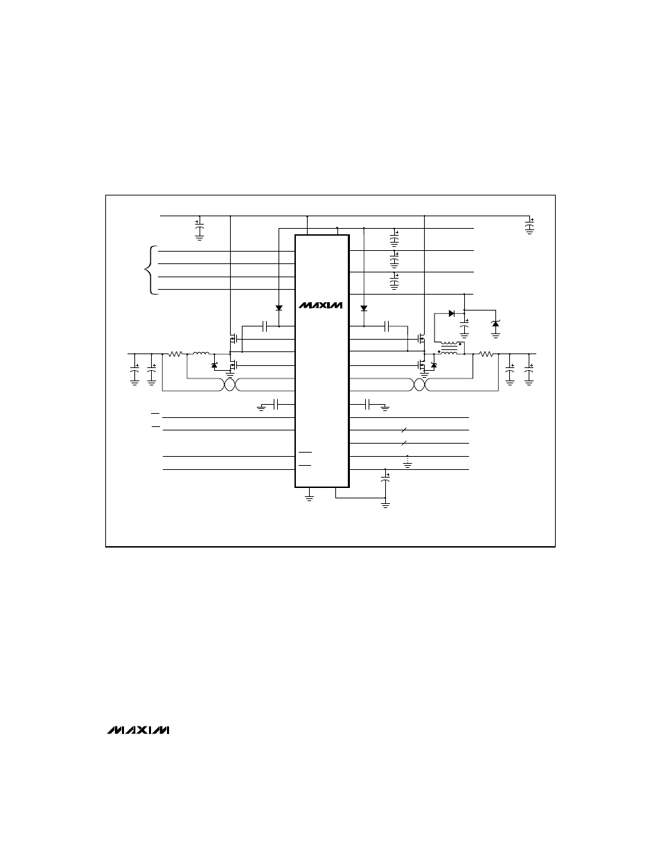
BATTERY INPUT
5.5V TO 30V
(NOTE 1)
VPP
CONTROL
INPUTS
C1
33
µ
F
D1A
C10
N1
L1
10
µ
H
R1
25m
Ω
+5V
at
3A
C3
330
µ
F
C4
330
µ
F
D2
1N5819
N2
C13
0.01
µ
F
+3.3V ON/OFF
+5V ON/OFF
SHUTDOWN
C15
1
µ
F
C7
4.7
µ
F
C8
1
µ
F
C9
1
µ
F
D1B
C11
0.1
µ
F
D3
EC11FS1
N3
1:4
L2 10
µ
H
D5
1N5819
N4
R2
20m
Ω
C12
2.2
µ
F
+3.3V
at
3A
C14
0.01
µ
F
2
2
COMPARATOR SUPPLY INPUT
COMPARATOR INPUTS
COMPARATOR OUTPUTS
OSCILLATOR SYNC
+5V at 5mA
0V, 3.3V, 5V, 12V
+15V AT 200mA, SEE
HIGH-SIDE SUPPLY (VDD)
SECTION.
0V, 3.3V, 5V, 12V
MAX783
V+
VL
C2
33
µ
F
C1–C6 = SPRAGUE 595D or AVX TPS SERIES
N1–N4 = Si9410DY or IRF7101 (BOTH SECTIONS)
D1A, D1B = LOW-POWER SCHOTTKY (CMPSH3 OR EQUIVALENT)
FOR V
+ <
6V. FOR V
+ >
6V, 1N4148 OR EQUIVALENT IS ACCEPTABLE.
NOTE 1: BATTERY VOLTAGE RANGE 6V to 20V WITH COMPONENTS SHOWN.
NOTE 2: KEEP KELVIN-CONNECTED CURRENT-SENSE TRACES SHORT AND CLOSE TOGETHER. SEE FIG.5.
NOTE 3: ZENER DIODE CLAMP REQUIRED FOR VIN
>
12V. ZENER CAN BE REPLACED WITH 20k
Ω
PULL-DOWN OR OTHER 1mA MINIMUM LOAD.
(NOTE 2)
(NOTE 2)
0.1
µ
F
D6
18V
100mW (NOTE 3)
C5
150
µ
F
C6
150
µ
F
3.3V AT 5mA
5V POWERGOOD
SYNC
REF
RDY5
2
8
14
13
Figure 1. Standard Application Circuit