Max783, Detailed description – Rainbow Electronics MAX783 User Manual
Page 8

MAX783
_______________Detailed Description
The MAX783 converts a 5.5V to 30V input to six outputs
(Figure 1). It produces two high-power, PWM switch-
mode supplies, one at +5V and the other at +3.3V. The
two supplies operate at either 300kHz or 200kHz, allow-
ing for small external components. Output current capa-
bility depends on external components, and can exceed
6A on each supply. Two 12V VPP outputs, an internal 5V,
25mA supply (VL) and a 3.3V, 5mA reference voltage
are also generated via linear regulators (Figure 2). Fault-
protection circuitry shuts off the PWM and high-side sup-
ply when the internal supplies lose regulation.
Two precision voltage comparators are also included.
Their output stages permit them to be used as level
translators for driving external N-channel MOSFETs in
load-switching applications, or for more conventional
logic signals.
The MAX783 is capable of accepting input voltages
from 5.5V to 30V, but is optimized for the lower end of
this range because the +15V flyback winding controller
is appended to the +3.3V buck supply. This architecture
allows for lower input voltages than are possible with the
MAX782 sister chip, which puts the winding on the +5V
side, while maintaining high +15V load capability.
However, the MAX783’s transformer has a higher turns
ratio (4:1 vs. 2:1), which leads to higher interwinding
capacitance as well as higher switching noise ampli-
tudes at the transformer secondary when the input volt-
age is high. Therefore, the MAX783 standard applica-
tion circuit is optimized with external components for
low-voltage (6-8 cell) designs with maximum input volt-
ages of 20V and less. The MAX783 itself can easily
accept 30V inputs, but expect to see more noise and
higher voltage swings at the transformer secondary
under these conditions. The inductor and filter capacitor
values may also require some adjustment for inputs
greater than 20V; see the
Design Procedure section.
+5V Switch-Mode Supply
The +5V supply is generated by a current-mode PWM
step-down regulator using two N-channel MOSFETs, a
rectifier, plus an LC output filter (Figure 1). The gate-
drive signal to the high-side MOSFET, which must
exceed the battery voltage, is provided by a boost cir-
cuit that uses a 100nF capacitor connected to BST5.
The +5V supply’s dropout voltage, as configured in
Figure 1, is typically 400mV at 2A. As V+ approaches
5V, the +5V output falls with V+ until the VL regulator
output hits its undervoltage lockout threshold at 4V. At
this point, the +5V supply turns off.
A synchronous rectifier at LX5 keeps efficiency high by
effectively clamping the voltage across the rectifier
diode. Maximum current limit is set by an external low-
value sense resistor, which prevents excessive inductor
current during start-up or under short-circuit conditions.
Programmable soft-start is set by an optional external
capacitor; this reduces in-rush surge currents upon
start-up and provides adjustable power-up times for
power-supply sequencing purposes.
+3.3V Switch-Mode Supply
The +3.3V output is produced by a current-mode PWM
step-down regulator similar to the +5V supply. The +3.3V
supply uses a transformer primary winding as its induc-
tor; the secondary is used for the 15V VDD supply.
The default switching frequency for both PWM controllers
is 200kHz (with SYNC connected to GND or VL), but
300kHz may be used by connecting SYNC to REF.
+3.3V and +5V PWM Buck Controllers
The two current-mode PWM buck controllers are nearly
identical except for different preset output voltages and
the addition of a flyback winding control loop to the
3.3V side. Each PWM is independent, except both are
synchronized to a master oscillator and share a com-
mon reference (REF) and logic supply (VL). Each PWM
can be turned on and off separately via ON3 and ON5.
The PWMs are a direct-summing type, lacking a tradi-
tional integrator-type error amplifier and the phase shift
associated with it. They therefore do not require exter-
nal feedback compensation components if you follow
the filter capacitor ESR guidelines in the
Design
Procedure.
The main gain block is an open-loop comparator that
sums four input signals: output voltage error signal,
current-sense signal, slope-compensation ramp, and
precision reference voltage. This direct-summing
method approaches the ideal of cycle-by-cycle control
of the output voltage. Under heavy loads, the controller
operates in full PWM mode. Every pulse from the oscil-
lator sets the output latch and turns on the high-side
switch for a period determined by the duty factor
(approximately V
OUT
/V
IN
). As the high-side switch turns
off, the synchronous rectifier latch is set; 60ns later, the
low-side switch turns on. The low-side switch stays on
until the beginning of the next clock cycle (in continu-
ous mode) or until the inductor current crosses through
Triple-Output Power-Supply Controller
for Notebook Computers
8
_______________________________________________________________________________________
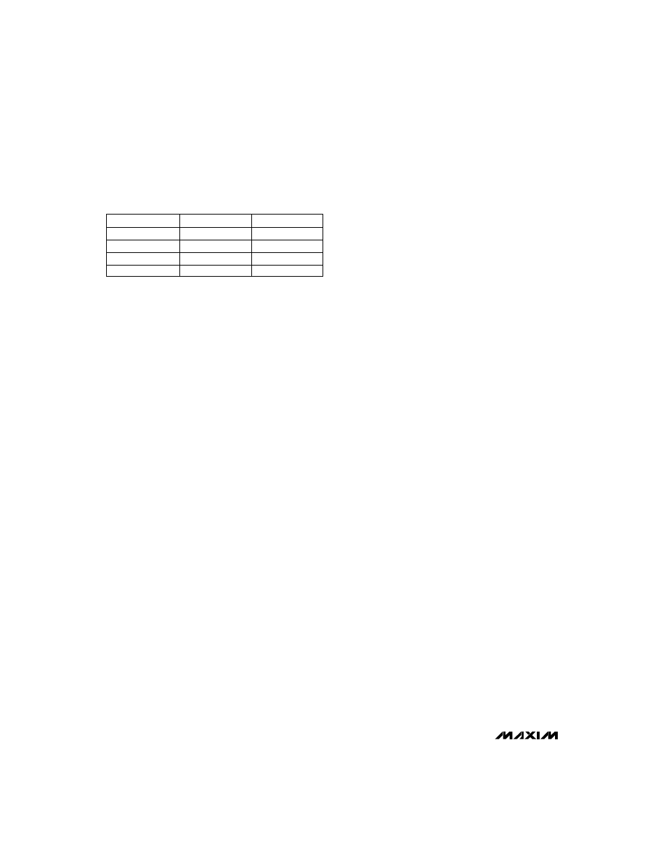
Table 1. Truth Table for VPP Control Pins
D_0
D_1
VPP
0
0
0V
0
1
5V
1
0
12V
1
1
3.3V
