Pin description – Rainbow Electronics MAX783 User Manual
Page 7
MAX783
Triple-Output Power-Supply Controller
for Notebook Computers
_______________________________________________________________________________________
7
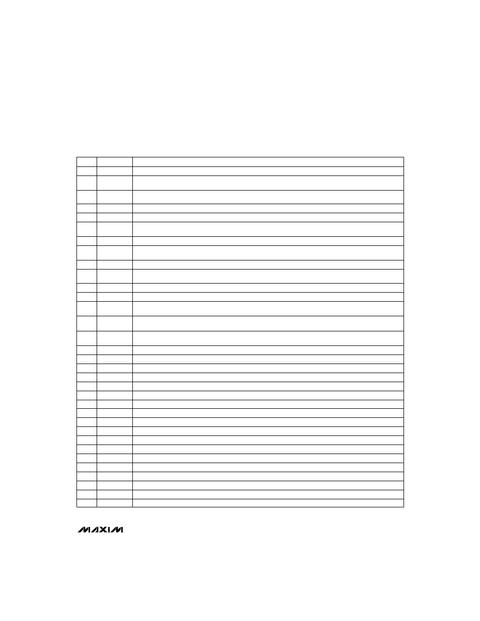
NAME
FUNCTION
1
ON3
ON/O
—
F
—
F
–
control input to disable the +3.3V PWM. Tie directly to VL for automatic start-up.
2
S
—
H
—
D
—
N
–
PIN
______________________________________________________________Pin Description
3
D1
4
D2
#2 level-translator/comparator noninverting input (see D1).
8
R
—
D
—
Y
—
5
–
7
Q1
#1 level translator/comparator output (see Q2).
6
Q2
5
VH
External positive supply voltage input for the level translators/comparators and R
—
D
—
Y
—
5
–
output.
19
ON5
ON/O
—
F
—
F
–
control input to disable the +5V PWM supply. Tie to VL for automatic start-up.
PCMCIA digital control inputs with industry-standard coding (see Table 1).
14
SYNC
13
REF
12
GND
Low-current analog ground. Feedback reference point for all outputs.
11
VPPB
0V, 3.3V, 5V, 12V switchable PCMCIA VPP output. Sources 60mA. Controlled by DB0 and DB1.
10
VDD
9
VPPA
0V, 3.3V, 5V, 12V switchable PCMCIA VPP output. Sources 60mA. Controlled by DA0 and DA1.
20
SS5
Soft-start control input for +5V. Ramp time to full current limit is 1ms/nF of capacitance to GND.
21
CS5
Current-sense input for +5V. Current limit level is +100mV referred to FB5.
22
DH5
Gate-drive output for the +5V high-side MOSFET.
23
LX5
Inductor connection for the +5V supply.
24
BST5
Boost capacitor connection for the +5V supply (0.1µF).
25
DL5
Gate-drive output for the +5V low-side MOSFET.
26
PGND
Power ground
15-18
27
FB5
Feedback and current-sense input for the +5V PWM.
29
V+
Supply voltage input from battery, 5.5V to 30V
28
VL
5V logic supply voltage for internal circuitry. VL is always on and can source 5mA for external loads.
33
DH3
Gate-drive output for the +3.3V high-side MOSFET.
32
LX3
Inductor connection for the +3.3V supply.
31
BST3
Boost capacitor connection for the +3.3V supply (0.1µF).
30
DL3
Gate-drive output for the +3.3V low-side MOSFET.
36
SS3
Soft-start input for +3.3V. Ramp time to full current limit is 1ms/nF of capacitance to GND.
35
CS3
Current-sense input for +3.3V, current limit level is +100mV referred to FB3.
34
FB3
Feedback and current-sense input for the +3.3V PWM.
DA1, DA0,
DB1, DB0
Shutdown control input, low-true logic. Tie to VL for automatic start-up. The 5V VL supply stays active in
shutdown. Don't force S
—
H
—
D
—
N
–
higher than VL + 0.5V.
#2 level-translator/comparator output. Sources 20µA from VH when D2 is high. Sinks 500µA to GND when
D2 is low, even with VH = 0V.
Power-good indication for the main +5V supply. Low indicates greater than 4.5V at the +5V output.
Swings 0V to VH.
+15V flyback input (feedback). A weak shunt regulator conducts 3mA to GND when VDD exceeds 19V.
VDD serves as the supply input for the VPP linear regulators.
3.3V reference output sources up to 5mA for external loads. Bypass to GND with 1µF/mA of load or
0.22µF minimum
Oscillator control/synchronization input. Connect to VL or GND for 200kHz; connect to REF for 300kHz.
For external clock synchronization in the 240kHz to 350kHz range, a high-to-low transition starts a new cycle.
#1 level-translator/comparator noninverting input, threshold = +1.650V. Controls Q1. Tie to GND if
unused.