Max783 – Rainbow Electronics MAX783 User Manual
Page 16
MAX783
Ensure the transformer secondary is connected with the
right polarity: A VDD supply will be generated with either
polarity, but proper operation is possible only with the cor-
rect polarity. Test for correct connection by observing the
phase relationship between the LX3 switching node and
the transformer secondary under load. The two wave-
forms must be 180° out of phase.
Current-Sense Resistors (R1, R2)
The sense resistors must carry the peak current in the
inductor, which exceeds the full DC load current.
The internal current limiting starts when the voltage
across the sense resistors exceeds 100mV nominally,
80mV minimum. Use the minimum value to ensure
adequate output current capability: For the +5V sup-
ply, R1 = 80mV / (1.15 x I
OUT
); for the +3.3V supply,
R2 = 80mV/(1.15 x I
TOTAL
), assuming that LIR = 0.3.
Since the sense resistance values (e.g., R1 = 25m
Ω
for
I
OUT
= 3A) are similar to a few centimeters of narrow
traces on a printed circuit board, trace resistance can
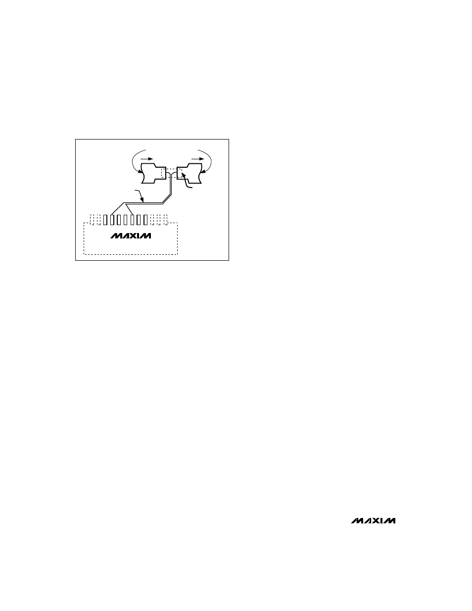
contribute significant errors. To prevent this, Kelvin
connect the CS_ and FB_ pins to the sense resistors;
use separate traces not carrying any of the inductor or
load current, as shown in Figure 5. Run these traces
parallel at minimum spacing from one another. The
wiring layout for these traces is critical for stable, low-
ripple outputs (see the
Layout and Grounding section).
MOSFET Switches (N1-N4)
The four N-channel power MOSFETs are usually identi-
cal and must be “logic-level” FETs; that is, they must be
fully on (have low r
DS(ON)
) with only 4V gate-source
drive voltage. The MOSFET r
DS(ON)
should ideally be
about twice the value of the sense resistor. MOSFETs
with even lower r
DS(ON)
have higher gate capacitance,
which increases switching time and transition losses.
MOSFETs with low gate-threshold voltage specifica-
tions (i.e., maximum V
GS(TH)
= 2V rather than 3V) are
preferred, especially for high-current (5A) applications.
Output Filter Capacitors (C3–C6)
The output filter capacitors determine the loop stability
and output ripple voltage. To ensure stability, the mini-
mum capacitance and maximum ESR values are:
V
REF
C
F
> —————————————
(V
OUT
) (R
CS
) (2) (
π
) (GBWP)
and,
(V
OUT
) (R
CS
)
ESR
CF
< ——————
V
REF
where:
C
F
= output filter capacitance, C6 or C7 (F)
V
REF
= reference voltage, 3.3V
V
OUT
= output voltage, 3.3V or 5V
R
CS
= sense resistor (
Ω
)
GBWP = gain-bandwidth product, 60kHz
ESR
CF
= output filter capacitor ESR (
Ω
).
Be sure to select output capacitors that satisfy
both
the
minimum capacitance and maximum ESR require-
ments. To achieve the low ESR required, it may be
appropriate to use a capacitance value 2 or 3 times
larger than the calculated minimum.
The output ripple in continuous-current mode is:
V
OUT(RPL)
= (I
LPP(MAX)
) [(ESR
CF
+1/(2 x
π
x f x C
F
)].
In idle-mode, the ripple has a capacitive and resistive
component:
(4 x 10
-4
) (L)
V
OUT(RPL)
(C) = ——————— x
(R
CS
2
) (C
F
)
1 1
(
——— + —————
)
Volts
V
OUT
V
IN
- V
OUT
(0.02) (ESR
CF
)
V
OUT(RPL)
(R) = ——————- Volts
R
CS
The total ripple, V
OUT(RPL)
, can be approximated as fol-
lows:
if V
OUT(RPL)
(R) < 0.5 V
OUT(RPL)
(C),
then V
OUT(RPL)
= V
OUT(RPL)
(C),
otherwise, V
OUT(RPL)
= 0.5 V
OUT(RPL)
(C) +
V
OUT(RPL)
(R).
Triple-Output Power-Supply Controller
for Notebook Computers
16 _______________________________________________________________________________________
MAX783
KELVIN SENSE TRACES
SENSE RESISTOR
MAIN CURRENT PATH
FAT, HIGH-CURRENT TRACES
Figure 5. Kelvin Connections for the Current-Sense Resistors