Esd protection, Data transfer – Rainbow Electronics MAX3345E User Manual
Page 9
MAX3344E/MAX3345E
±15kV ESD-Protected USB Transceivers
in UCSP with USB Detect
_______________________________________________________________________________________
9
Data Transfer
Receiving Data from the USB
Data received from the USB are output to VPI/VMI in
either of two ways, differentially or single ended. To
receive data from the USB, force
OE high and SUSP low.
Differential data arriving at D+/D- appear as differential
logic signals at VPI/VMI, and as a single-ended logic sig-
nal at RCV. If both D+ and D- are low, then VPI and VMI
are low, signaling a single-ended zero condition on the
bus; RCV remains in the last known state (Table 3).
Transmitting Data to the USB
The MAX3344E/MAX3345E output data to the USB dif-
ferentially on D+ and D-. The logic driving signals can
be either differential or single ended. For sending differ-
ential logic, force MODE high, force
OE and SUSP low,
and apply data to VPO and VMO. D+ then follows VPO,
and D- follows VMO. To send single-ended logic sig-
nals, force MODE, SUSP, and
OE low, and apply data to
VPO/VMO.
ESD Protection
To protect the MAX3344E/MAX3345E against ESD, D+
and D- have extra protection against static electricity to
protect the device up to ±15kV. The ESD structures
withstand high ESD in all states—normal operation,
suspend, and powered down. For the 15kV ESD struc-
tures to work correctly, a 1µF or greater capacitor must
be connected from VTRM to GND.
ESD protection can be tested in various ways; the D+
and D- input/output pins are characterized for protection
to the following limits:
1) ±15kV using the Human Body Model
2) ±8kV using the IEC 1000-4-2 Contact Discharge
Method
3) ±10kV using the IEC 1000-4-2 Air-Gap Method
ESD Test Conditions
ESD performance depends on a variety of conditions.
Contact Maxim for a reliability report that documents test
setup, test methodology, and test results.
Human Body Model
Figure 1a shows the Human Body Model, and Figure 1b
shows the current waveform it generates when dis-
charged into a low impedance. This model consists of a
100pF capacitor charged to the ESD voltage of interest,
which is then discharged into the test device through a
1.5kΩ resistor.
D+/D-
t
PDZ
t
PZD
V
OHD
- 0.3V
V
OLD
+ 0.3V
V
L
0V
V
L
/2
OE
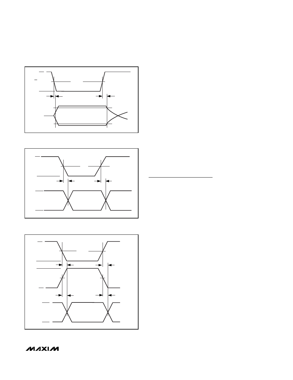
Figure 2. Enable and Disable Timing, Transmitter
VPO
t
PHLO
V
L
0V
D+
D-
0V
VTRM
V
L
/2
t
PLHO
Figure 3. Mode 0 Timing
t
PLH1
V
L
0V
0V
VTRM
V
L
/2
D+
D-
VMO
V
L
0V
t
PHL1
V
L
/2
t
PLH1
t
PLH1
V
L
/2
VPO
Figure 4. Mode 1 Timing