Rainbow Electronics DS1616 User Manual
Page 8
DS1616
8 of 28
The thermal sensor is enabled by setting the CS0 bit of the Control 2 register to a logic 1. If the CS0 bit
is a logic 0, the thermal sensor will not be activated during a datalogging mission or for an individual
Read Data command. If CS0 = 0, the value in the Current Temperature register will be 11111111b.
The format of temperature data is defined such that the temperature value is maintained in a single byte of
data. Table 1 illustrates the format of the temperature data byte format. The values of T[7..0] range from
00000000b (for -40
°C) to 11111010b (for +85°C). Each increment in the value of T[7..0] represents an
increase in temperature of 0.5
°C. The following formula can be used to translate the temperature data
byte value into degrees Celsius:
°C = 0.5(T[7..0]) - 40
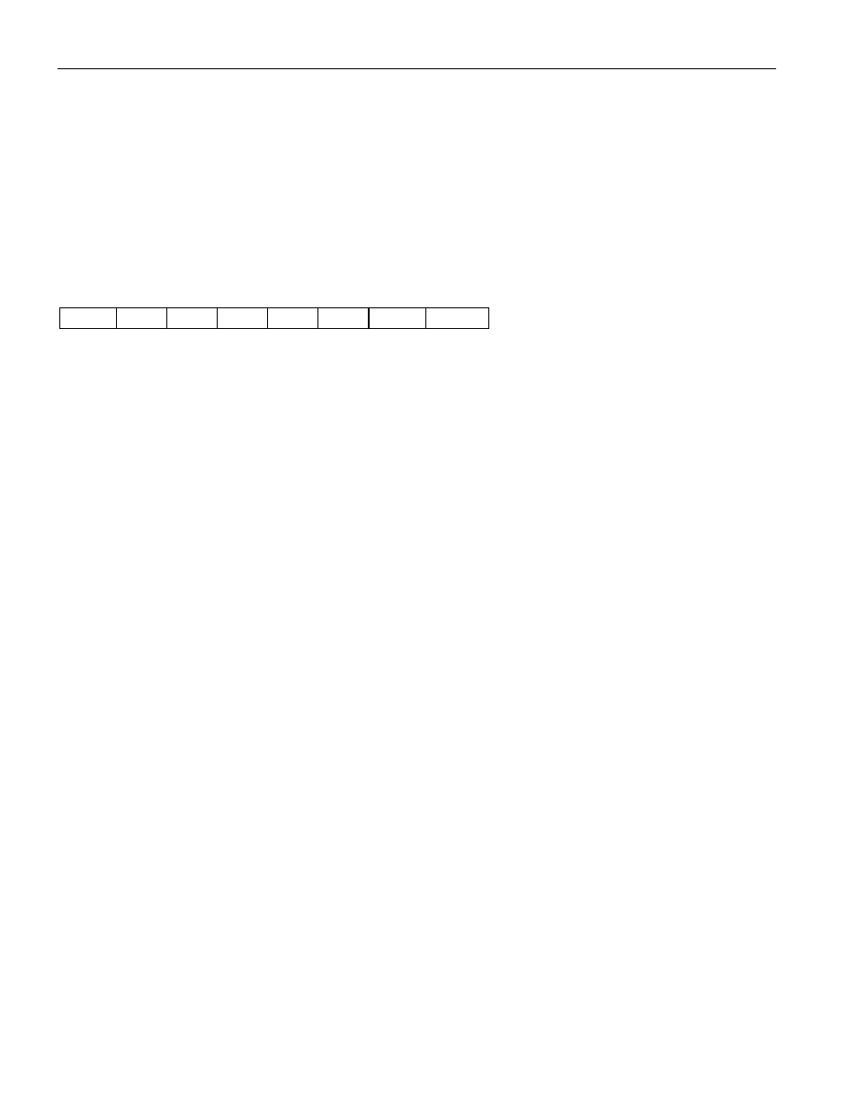
TEMPERATURE DATA BYTE FORMAT Table 1
MSb
LSb
T7
T6
T5
T4
T3
T2
T1
T0
When a datalog mission has been initiated and the thermal sensor is enabled (CS0=1), the DS1616
provides temperature recording at regular intervals. However, the device also allows for immediate
temperature sensing upon a user’s command when the device is not currently on a datalog mission and
the thermal sensor is enabled (CS0=1). This is accomplished by issuing the Read Data command to the
DS1616 over the serial interface.
The most recently recorded temperature value is written to the Current Temperature register, regardless of
whether that value was recorded from a datalog mission or from the issuance of the Read Data command.
The status of the contents of this register is provided by the Data Ready (DR) bit in the Status 1 register.
If DR is a logic 1, the data is valid. If DR is a logic 0, the data may not be reliable. If CS0 in the Control
2 register is a 0 such that the thermal sensor is disabled, the value in the Current Temperature register will
be 11111111b. The Read Data command will not output this byte of data.
During a datalog mission, the DR bit is cleared to a logic 0 when a temperature conversion has been
initiated and is set to a logic 1 upon the completion of the conversion. Likewise, the DR bit is cleared
immediately after the Read Data command is issued and is set to a logic 1 upon the completion of the
conversion. The Read Data command will only read the values in the current temperature/ADC data that
have been enabled by the CSx[03] bits in the control 2 register.
ANALOG-TO-DIGITAL CONVERTER (ADC)
The DS1616 contains an integrated 8-bit ADC with a 3 to 1 input mux to allow multiple sensors to be
monitored. An on-chip voltage reference is also provided by an integrated band gap circuit (2.04V
±3%).
The ADC input voltage must not be greater than the battery voltage.
An analog-to-digital conversion is the process of assigning a digital value to an analog input voltage.
This code represents the input value as a fraction of the full scale voltage (FSV) range. Thus the FSV
range is then divided by the ADC into 256 codes (8 bits). The FSV range is bounded by an upper limit
equal to the reference voltage and the lower limit, which is ground. The 2.04V (typical) bandgap
reference provides a resolution of 8mV between codes.
An input voltage equal to the reference voltage converts to FFh while an input voltage equal to ground
converts to 00h. The relative linearity of the ADC is
±0.5 LSB.
When a datalog mission has been initiated and one or more of the Analog Inputs are enabled (CS[1-3] =
1), the DS1616 provides data conversion and recording at regular intervals. However, the device also