Figure 6. current-sense amplifier response, Undervoltage lockout (uvlo), Internal oscillator and clock generation – Rainbow Electronics DS2712 User Manual
Page 9: Current-sense amplifier (ds2711), Current-sense comparator (ds2712)
DS2711/DS2712: Loose Cell NiMH Charger
9 of 13
Undervoltage Lockout (UVLO)
The UVLO circuit serves as a power-up and brownout detector by monitoring V
DD
to prevent charging until V
DD
rises above V
UVLO
, or when V
DD
drops below V
UVLO
- V
HYS
. If UVLO is active, charging is prevented, the state
machine is forced to the RESET state, and all charge timers are reset. A 10
ms deglitch circuit provides noise
immunity.
Internal Oscillator and Clock Generation
An internal oscillator provides the main clock source used to generate timing signals for internal chip operation. The
precharge timer, hold-off timers, and timings for CC1/CC2 operation and cell testing are derived from this timebase.
In case the internal clock should ever fail, a watchdog detection circuit halts charging. The watchdog safety circuit
and charge timer set by the TMR pin are derived from separate oscillators than the main clock source.
Current-Sense Amplifier (DS2711)
An error amplifier block provides several options to regulate the charge current. The 20mA open-drain output can
drive a PMOS or PNP pass element for linear regulation, or the output can drive an optocoupler for isolated
feedback to a primary-side PWM controller. The VN0 pin is a remote-sense return and should be connected to the
grounded side of the sense resistor using a separate, insulated conductor.
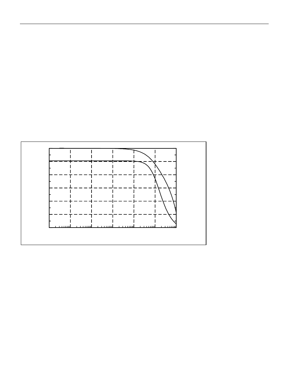
Figure 6. Current-Sense Amplifier Response
The open-loop amplifier response shown in Figure 6 was measured with I
CSOUT
= -1mA. An error signal between
the current-sense signal (across a sense resistor) and the 0.125V internal reference is produced so the voltage
across the sense resistor is maintained at V
IREF
in a closed-loop circuit.
Current-Sense Comparator (DS2712)
The comparator in the DS2712 switches between ON and OFF and is capable of driving a PNP bipolar or a PMOS
transistor, enabling the use of a switched-mode power stage. Hysteresis on the comparator input provides noise
rejection. In the closed-loop regulation circuit of Figure 5, the comparator regulates voltage across the sense
resistor to a DC average of:
V
RSNS
= V
IREF
- 0.5 x V
HYS-COMP
= 0.125V
Frequency (Hertz)
10
1
10
2
10
3
10
4
10
5
10
6
10
7
Ga
in
0.00
0.20
0.40
0.60
0.80
1.00
1.20
Phase
-300
-250
-200
-150
-100
-50
0
Gain
Phase