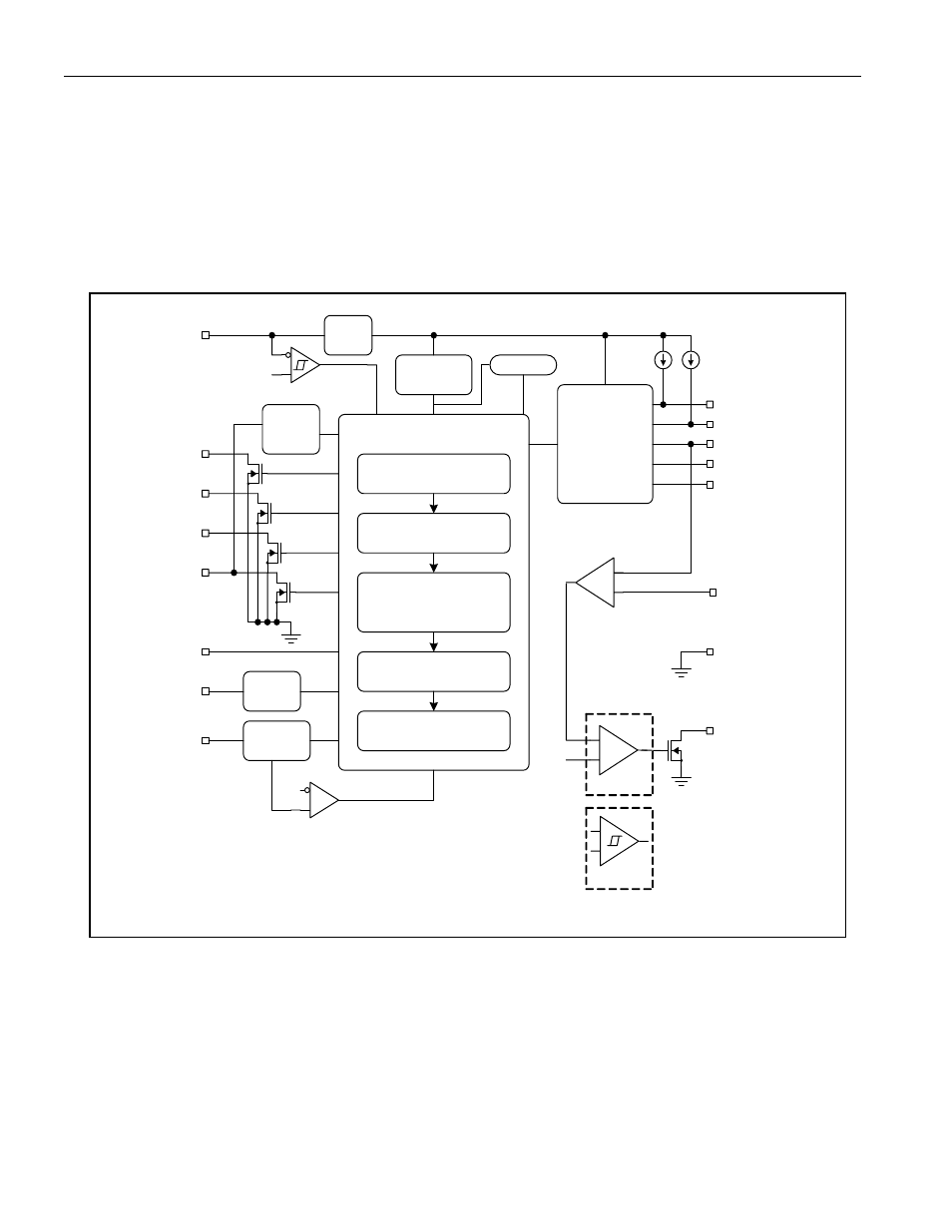
Figure 1. block diagram, Ctst cc1 csout, Dmsel – Rainbow Electronics DS2712 User Manual
Page 4
DS2711/DS2712: Loose Cell NiMH Charger
4 of 13
Note 1:
Voltages relative to V
SS
.
Note 2:
I
MTST
current is applied as a source current and as a sink current within 5ms after power-up.
Note 3:
When operating in two-cell-series charge configuration, the DMSEL pin must have less than 50pF of external load capacitance
for proper operation. If the load capacitance is greater than 50pF, a resistor voltage divider should be used to maintain DMSEL
at V
DD
/ 2.
Note 4:
Specification applicable during charge cycle with T
A
= 0
°C to +70°C.
Note 5:
V
BAT-MAX1
and V
BAT-MAX1
are generated from the same reference. Their ranges never overlap.
Note 6:
V
THM-MIN,
V
THM-MAX,
and
V
THM-STOP
are fixed ratios of V
DD.
Their ranges never overlap.
Note 7:
Tested with I
CSOUT
= -1mA.
Note 8:
Gain tested with 1mV step with I
CSOUT
= -1mA.
Figure 1. BLOCK DIAGRAM
+
-
State Machine
Voltage
and
Temperature
Measurement
Charge
Timer
BIAS
VP1
CC2
LED1
TMR
VDD
VSS
LED2
VP2
THM1
THM2
Cell
Test
CTST
CC1
CSOUT
0.125V
DMSEL
SUSPEND
3.7V
UVLO
Oscillator
+
-
VN0
Presence Test
Pre-Charge
Fast Charge
&
Cell Tests
Top-Off Charge
Maintenance Charge
Charge
Mode
Select
VN1
Watchdog
+
-
AB
O
R
T
I
PTST
I
PTST
0.1V
DS2712
DS2711