Ds4426 quad-channel, i, Power-supply tracking circuit – Rainbow Electronics DS4426 User Manual
Page 7
DS4426
Quad-Channel, I
2
C-Margining IDACs with
Three Channels of Power-Supply Tracking
_______________________________________________________________________________________
7
Using the external resistors R
FS[3:0]
to set the output-
current range, the DS4426 provides some flexibility for
adjusting the impedances of the feedback network or
the range over which the power supply can be con-
trolled or margined.
As a source for biasing instrumentation or other circuits,
the DS4426 provides a simple and inexpensive current
source with an I
2
C interface for control. The adjustable,
full-scale range allows the application to get the most
out of its 7-bit sink or source resolution.
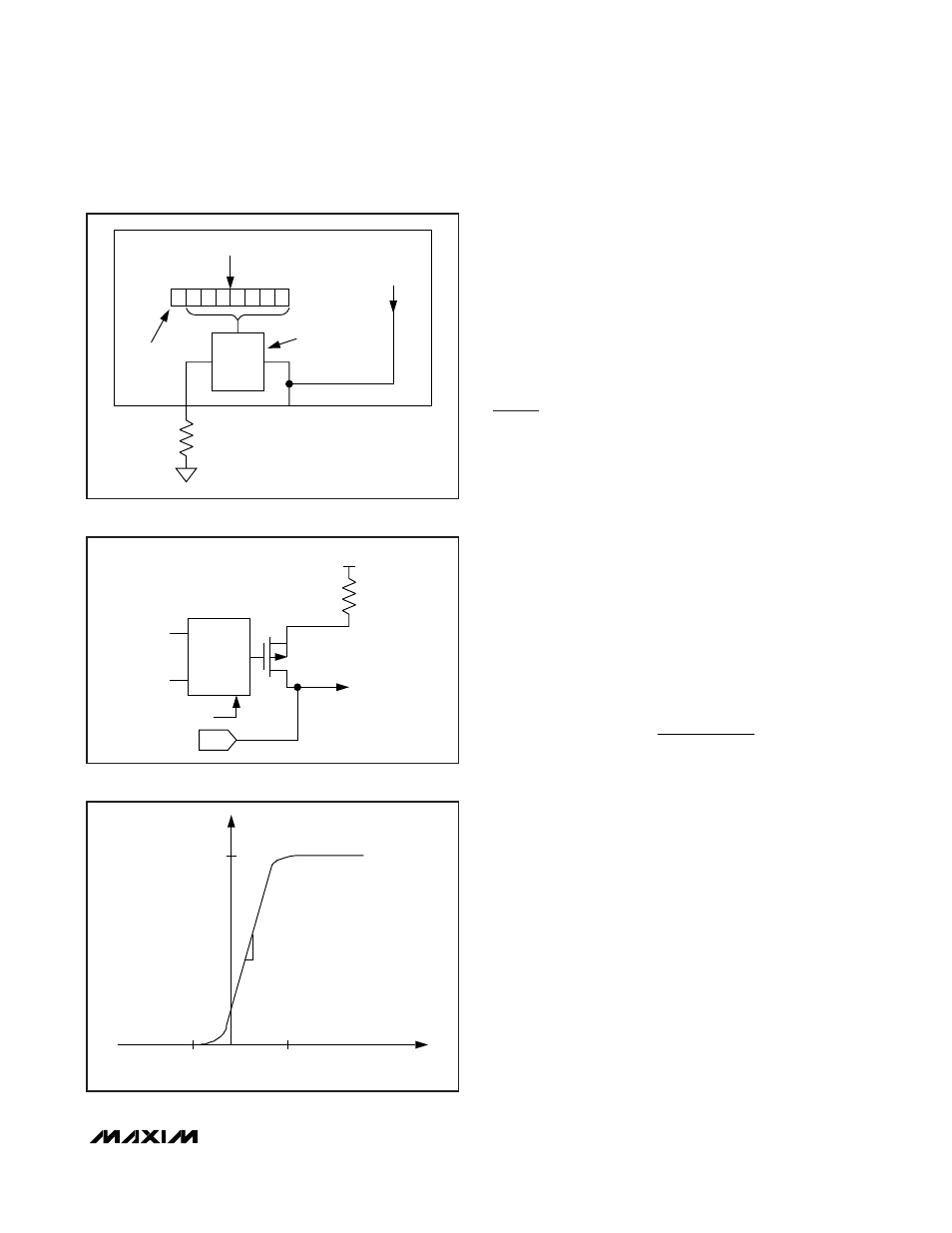
Power-Supply Tracking Circuit
By making use of the power-supply tracking circuitry,
the DS4426 has the ability to source current on power-
up. This current is additive with the current DAC
source/sink currents and is determined by the value of
the gain resistor, R
G
, and the supply voltage, V
CC
. This
current is controlled by the voltages presented to the
corresponding INP and INN pins, and the voltages pre-
sented to the corresponding threshold (THR) pins.
Maximum Source Current
The maximum current the DS4426 can source at
power-up using the power-supply tracking circuitry
depends on the value of the supply voltage, V
CC
, and
the gain resistor, R
G
, connected from the correspond-
ing GAIN pin to V
CC
. The maximum current (I
MAX
) that
can be sourced to the corresponding OUT pin can be
estimated using the following equation:
The power-supply tracking circuit can be estimated
with Figure 2.
Inputs for Power-Supply Tracking:
INP and INN
Each pair of power-supply tracking inputs, INP and
INN, determines if and how much of the I
MAX
current is
sourced when the power-supply tracking circuit is
enabled. When the difference between the voltage pre-
sented to INP (V
INP
) and INN (V
INN
) is more than
approximately +0.3V, then the maximum source cur-
rent, as determined by the value I
MAX
, is sourced into
the OUT pin connection. When the difference between
V
INP
and V
INN
is less than approximately -0.2V, then no
current is sourced into the corresponding OUT pin. The
change in current from no current to I
MAX
can be esti-
mated by the power-supply tracking gain, G
VI
(see the
Power-Supply Tracking Characteristics
table).
Figure 3 shows the typical current behavior of the
power-supply tracking circuit with respect to the volt-
age difference seen at the INP and INN inputs.
I
V
V
R
MAX
CC
OUT
G
≅
−
(
)
MSB
LSB
CURRENT
DAC[3:0]
OUT[3:0]
FS[3:0]
TRACKING
OUT[3:1] ONLY
I
2
C CONTROL
127 POSITIONS
EACH FOR SOURCE
AND SINK MODE
SOURCE
OR
SINK MODE
R
FS[3:0]
Figure 1. Current DAC Detail
+
INP
GAIN
V
CC
DAC
OUT
SLAVE
FEEDBACK
NODE
G
VI
R
G
-
INN
SHUTDOWN
Figure 2. Gain Stage
I
-0.2
+0.3
AT V
CC
= +5.0V
I
MAX
G
VI
V
(V
INP
- V
INN
)
Figure 3. INP and INN Differential Inputs