Ds4426 quad-channel, i, Detailed description, Pin description – Rainbow Electronics DS4426 User Manual
Page 6
Detailed Description
The DS4426 contains four I
2
C-adjustable current
sources that are each capable of sinking and sourcing
current. Three of the current outputs (OUT[3:1]) also
have power-supply tracking circuitry that allows addi-
tional current to be sourced during power-up.
Adjustable Current DACs
Each output (OUT[3:0]) has 127 sink and 127 source
settings that are programmed through the I
2
C interface.
The full-scale current ranges (and corresponding step
sizes) of the outputs are determined by external resis-
tors connected to the corresponding FS pins (see
Figure 1). The formula to determine the external resistor
values (R
FS
) for each output is given by:
where I
FS
is the desired full-scale current value, V
RFS
is
the R
FS
voltage (see the
DC Electrical Characteristics
table), and R
FS
is the external resistor value.
To calculate the output-current value (I
OUT
) based on the
corresponding DAC value (see Table 2 for correspond-
ing memory addresses), use the following equation:
On power-up, the DS4426 current DAC outputs are set
to zero current. This is done to prevent the device from
sinking or sourcing an incorrect current before the sys-
tem host controller has a chance to modify its setting.
Note, however, that if power-supply tracking is enabled
(see the
Power-Supply Tracking Circuit
section), then
the DS4426 can still source current at power-up.
When used in adjustable power-supply applications
(see Figure 8), the DS4426 does not affect the initial
power-up voltage of the supply because it defaults to
providing zero output current on power-up unless
power-supply tracking is enabled. As it sources or
sinks current into the feedback voltage node, it
changes the amount of output voltage required by the
regulator to reach its steady-state operating point.
I
DACValue dec
I
OUT
FS
=
×
(
)
127
R
V
I
FS
RFS
FS
=
Ч
Ч
16
127
DS4426
Quad-Channel, I
2
C-Margining IDACs with
Three Channels of Power-Supply Tracking
6
_______________________________________________________________________________________
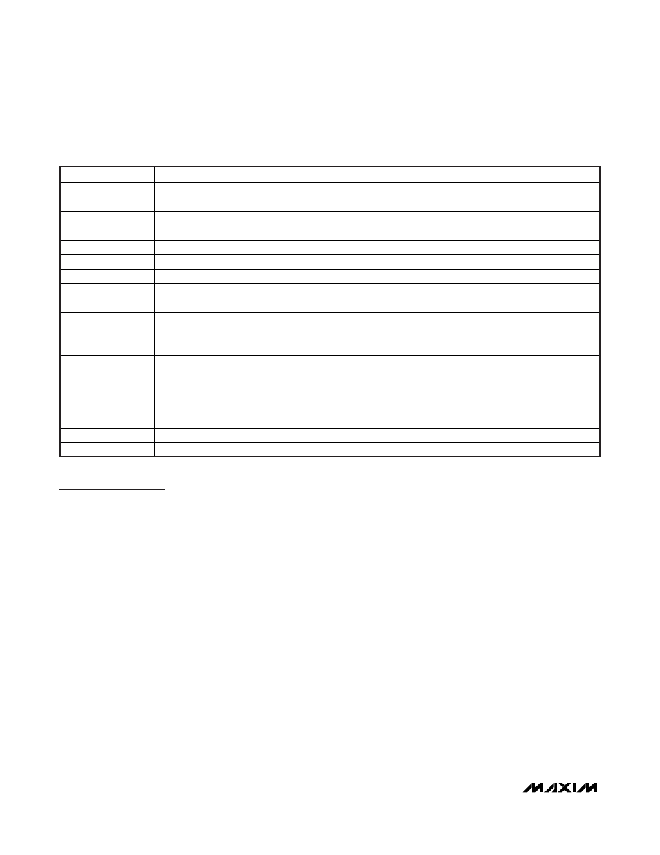
Pin Description
PIN
NAME
FUNCTION
1
SDA
Serial Data Input/Output. I
2
C data pin.
2
SCL
Serial Clock Input. I
2
C clock input.
3 V
CC
Voltage
Supply
4
OUT0
Current DAC Output
5, 6, 7
OUT1, OUT2, OUT3
Current DAC and Tracking Control Output
8 GND
Ground
9 A0
I
2
C Address Input 0
10 A1
I
2
C Address Input 1
11, 13, 15
INP1, INP2, INP3
Power-Supply Tracking Positive Input
12, 14, 16
INN1, INN2, INN3
Power-Supply Tracking Negative Input
17, 19, 20
THR3, THR2, THR1
Threshold Input. Comparator input used to set threshold for tracking
enable/disable based on V
REF
/2.
18
DNC
Do Not Connect
21–24
FS0, FS1, FS2, FS3
Full-Scale Calibration Input. A resistor-to-ground on this input determines full-
scale output current on the associated output.
25, 26, 27
GAIN3, GAIN2,
GAIN1
Gain Adjustment Pin. Connect a resistor between this pin and V
CC
.
28 N.C.
No
Connection
—
EP
Exposed Pad. No connection.