Table 3. trickle-charge register – Rainbow Electronics DS1340 User Manual
Page 9
Bit 6: Frequency Test (FT). When this bit is 1, the
FT/OUT pin toggles at a 512Hz rate. When FT is written
to 0, the OUT bit controls the state of the FT/OUT pin.
The initial power-up value of FT is 0.
Bit 5: Calibration Sign Bit (S). A logic 1 in this bit indi-
cates positive calibration for the RTC. A 0 indicates
negative calibration for the clock. See the Clock
Calibration section for a detailed description of the bit
operation. The initial power-up value of S is 0.
Bits 4 to 0: Calibration Bits (CAL4 to CAL0). These
bits can be set to any value between 0 and 31 in binary
form. See the Clock Calibration section for a detailed
description of the bit operation. The initial power-up
value of CAL0–CAL4 is 0.
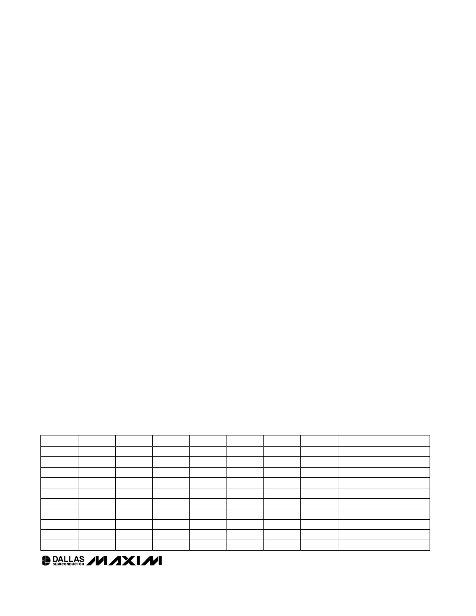
Trickle-Charger Register (08h)
The simplified schematic in Figure 6 shows the basic
components of the trickle charger. The trickle-charge
select (TCS) bits (bits 4–7) control the selection of the
trickle charger. To prevent accidental enabling, only a
pattern on 1010 enables the trickle charger. All other
patterns disable the trickle charger. The trickle charger
is disabled when power is first applied. The diode-
select (DS) bits (bits 2, 3) select whether or not a diode
is connected between V
CC
and V
BACKUP
. If DS is 01,
no diode is selected; if DS is 10, a diode is selected.
The ROUT bits (bits 0, 1) select the value of the resistor
connected between V
CC
and V
BACKUP
. Table 3 shows
the resistor selected by the resistor select (ROUT) bits
and the diode selected by the diode select (DS) bits.
Warning: The ROUT value of 250
Ω must not be select-
ed whenever V
CC
is greater than 3.63V.
The user determines diode and resistor selection
according to the maximum current desired for battery
or super cap charging (Table 3). The maximum charg-
ing current can be calculated as illustrated in the fol-
lowing example.
Assume that a 3.3V system power supply is applied to
V
CC
and a super cap is connected to V
BACKUP
. Also
assume that the trickle charger has been enabled with
a diode and resistor R2 between V
CC
and V
BACKUP
.
The maximum current I
MAX
would therefore be calculat-
ed as follows:
I
MAX
= (3.3V - diode drop) / R2
≈ (3.3V - 0.7V) /
2k
Ω ≈ 1.3mA
As the super cap charges, the voltage drop between
V
CC
and V
BACKUP
decreases and therefore the charge
current decreases.
Flag Register (09h)
Bit 7: Oscillator Stop Flag (OSF). A logic 1 in this bit
indicates that the oscillator has stopped or was
stopped for some time period and may be used to
judge the validity of the clock and calendar data. This
bit is edge triggered and is set to logic 1 when the
internal circuitry senses that the oscillator has transi-
tioned from a normal run state to a STOP condition. The
following are examples of conditions that can cause the
OSF bit to be set:
1)
The first time power is applied.
2)
The voltages present on V
CC
and V
BACKUP
are insufficient to support oscillation.
3)
The EOSC bit is set to 1, disabling the
oscillator.
4)
External influences on the crystal (e.g., noise,
leakage).
The OSF bit remains at logic 1 until written to logic 0. It
can only be written to logic 0. Attempting to write OSF
to logic 1 leaves the value unchanged.
DS1340
2-Wire RTC with Trickle Charger
_____________________________________________________________________
9
TCS3
TCS2
TCS1
TCS0
DS1
DS0
ROUT1
ROUT0
FUNCTION
X
X
X
X
0
0
X
X
Disabled
X
X
X
X
1
1
X
X
Disabled
X
X
X
X
X
X
0
0
Disabled
1
0
1
0
0
1
0
1
No diode, 250
Ω resistor
1
0
1
0
1
0
0
1
One diode, 250
Ω resistor
1
0
1
0
0
1
1
0
No diode, 2k
Ω resistor
1
0
1
0
1
0
1
0
One diode, 2k
Ω resistor
1
0
1
0
0
1
1
1
No diode, 4k
Ω resistor
1
0
1
0
1
0
1
1
One diode, 4k
Ω resistor
0
0
0
0
0
0
0
0
Power-on reset value
Table 3. Trickle-Charge Register