Ds1340, Wire rtc with trickle charger, Clock and calendar – Rainbow Electronics DS1340 User Manual
Page 8: Special-purpose registers
DS1340
the control register is located at 07h. The trickle-charge
and flag registers are located in address locations 08h
to 09h. During a multibyte access of the timekeeping
registers, when the address pointer reaches 07h—the
end of the clock and control register space—it wraps
around to location 00h. Writing the address pointer to
the corresponding location accesses address locations
08h and 09h. After accessing location 09h, the address
pointer wraps around to location 00h. On a 2-wire
START, STOP, or address pointer incrementing to loca-
tion 00h, the current time is transferred to a second set
of registers. The time information is read from these
secondary registers, while the clock may continue to
run. This eliminates the need to reread the registers in
case the main registers update during a read.
Clock and Calendar
The time and calendar information is obtained by read-
ing the appropriate register bytes. Table 2 shows the
RTC registers. The time and calendar data are set or
initialized by writing the appropriate register bytes. The
contents of the time and calendar registers are in the
binary-coded decimal (BCD) format. The day-of-week
register increments at midnight. Values that correspond
to the day of week are user-defined but must be
sequential (i.e., if 1 equals Sunday, then 2 equals
Monday, and so on). Illogical time and date entries
result in undefined operation. Bit 7 of register 0 is the
enable oscillator (
EOSC) bit. When this bit is set to 1, the
oscillator is disabled. When cleared to 0, the oscillator is
enabled. The initial power-up value of EOSC is 0.
Location 02h is the century/hours register. Bit 7 and bit
6 of the century/hours register are the century-enable
bit (CEB) and the century bit (CB). Setting CEB to logic
1 causes the CB bit to toggle, either from a logic 0 to a
logic 1, or from a logic 1 to a logic 0, when the years
register rolls over from 99 to 00. If CEB is set to logic 0,
CB does not toggle.
When reading or writing the time and date registers,
secondary (user) buffers are used to prevent errors
when the internal registers update. When reading the
time and date registers, the user buffers are synchro-
nized to the internal registers on any START or STOP
and when the register pointer rolls over to zero. The
time information is read from these secondary registers
while the clock continues to run. This eliminates the
need to reread the registers in case the internal regis-
ters update during a read.
The divider chain is reset whenever the seconds regis-
ter is written. Write transfers occur on the acknowledge
from the DS1340. Once the divider chain is reset, to
avoid rollover issues, the remaining time and date reg-
isters must be written within one second.
Special-Purpose Registers
The DS1340 has three additional registers (control,
trickle charger, and flag) that control the RTC, trickle
charger, and oscillator flag output.
Control Register (07h)
Bit 7: Output Control (OUT). This bit controls the out-
put level of the FT/OUT pin when the FT bit is set to 0. If
FT = 0, the logic level on the FT/OUT pin is 1 if OUT = 1
and 0 if OUT = 0. The initial power-up OUT value is 1.
2-Wire RTC with Trickle Charger
8
_____________________________________________________________________
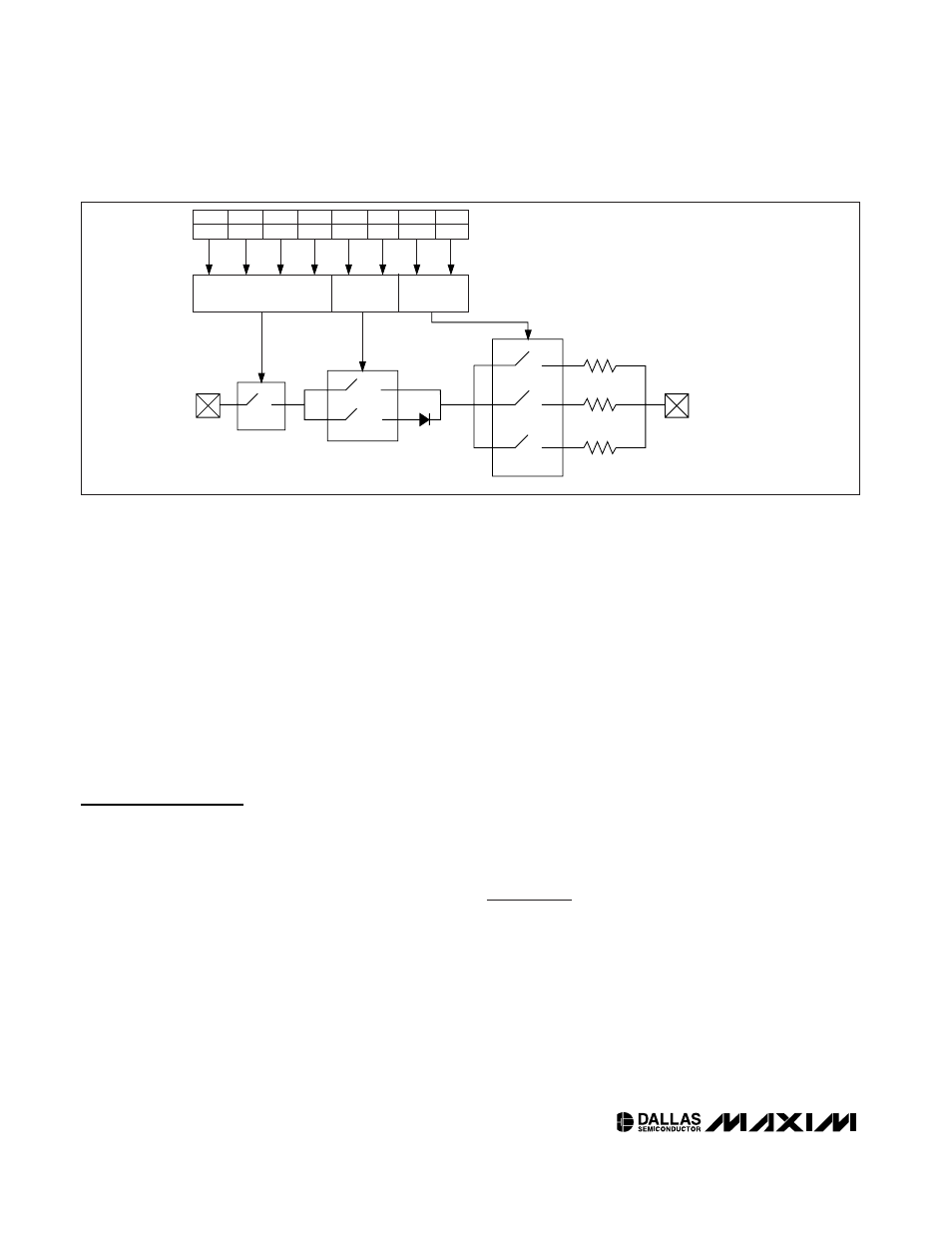
BIT 7
TCS3
1 OF 16 SELECT
NOTE: ONLY 1010b
ENABLES CHARGER
1 OF 2
SELECT
V
CC
V
BACKUP
R1
250
Ω
TCS
0-3
= TRICKLE-CHARGER SELECT
DS
0-1
= DIODE SELECT
TOUT
0-1
= RESISTOR SELECT
R2
2k
Ω
R3
4k
Ω
1 OF 3
SELECT
BIT 6
TCS2
BIT 5
TCS1
BIT 4
TCS0
BIT 3
DS1
BIT 2
DS0
BIT 1
ROUT1
BIT 0
ROUT0
Figure 6. Trickle Charger Functional Diagram