Ds1340, Wire rtc with trickle charger, Detailed description – Rainbow Electronics DS1340 User Manual
Page 6: Oscillator circuit, Clock accuracy, Pin description, Table 1. crystal specifications
DS1340
Detailed Description
The DS1340 is a low-power clock/calendar with a trickle
charger. Address and data are transferred serially
through a 2-wire bidirectional bus. The clock/calendar
provides seconds, minutes, hours, day, date, month, and
year information. The date at the end of the month is
automatically adjusted for months with fewer than 31
days, including corrections for leap year. The DS1340
has a built-in power-sense circuit that detects power fail-
ures and automatically switches to the backup supply.
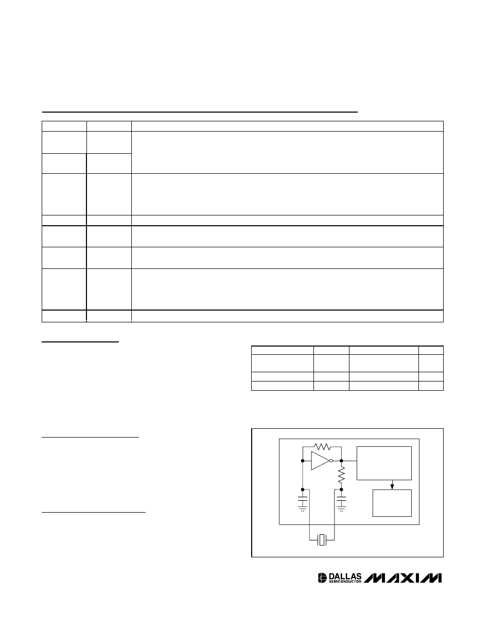
Oscillator Circuit
The DS1340 uses an external 32.768kHz crystal. The
oscillator circuit does not require any external resistors
or capacitors to operate. Table 1 specifies several crys-
tal parameters for the external crystal. Figure 3 shows a
functional schematic of the oscillator circuit. If using a
crystal with the specified characteristics, the startup
time is usually less than one second.
Clock Accuracy
The initial clock accuracy depends on the accuracy of
the crystal and the accuracy of the match between the
capacitive load of the oscillator circuit and the capaci-
tive load for which the crystal was trimmed. Additional
error is added by crystal frequency drift caused by
2-Wire RTC with Trickle Charger
6
_____________________________________________________________________
Pin Description
PIN
NAME
FUNCTION
1
X1
2
X2
Connections for a Standard 32.768kHz Quartz Crystal. The internal oscillator circuitry is designed for
operation with a crystal having a specified load capacitance (C
L
) of 12.5pF. X1 is the input to the
oscillator and can optionally be connected to an external 32.768kHz oscillator. The output of the
internal oscillator, X2, is floated if an external oscillator is connected to X1.
3
V
BACKUP
Connection for a Secondary Power Supply. For the 1.8V and 3V devices, V
BACKUP
must be held
between 1.3V and 3.7V for proper operation. V
BACKUP
can be as high as 5.5V on the 3.3V device.
This pin can be connected to a primary cell such as a lithium coin cell. Additionally, this pin can be
connected to a rechargeable cell or a super cap when used with the trickle-charge feature.
4
GND
Ground
5
SDA
Serial Data Input/Output. SDA is the data input/output for the 2-wire serial interface. The SDA pin is
open drain and requires an external pullup resistor.
6
SCL
Serial Clock Input. SCL is the clock input for the 2-wire interface and is used to synchronize data
movement on the serial interface.
7
FT/OUT
Frequency Test/Output. This pin is used to output either a 512Hz signal or the value of the OUT bit.
When the FT bit is logic 1, the FT/OUT pin toggles at a 512Hz rate. When the FT bit is logic 0, the
FT/OUT pin reflects the value of the OUT bit. This open-drain pin requires an external pullup resistor,
and operates with either V
CC
or V
BACKUP
applied.
8
V
CC
DC Power for Primary Power Supply
PARAMETER
SYMBOL
MIN
TYP
MAX
UNITS
Nominal
Frequency
f
O
32.768
kHz
Series Resistance
ESR
45
k
Ω
Load Capacitance
C
L
12.5
pF
Table 1. Crystal Specifications*
*The crystal, traces, and crystal input pins should be isolated
from RF generating signals. Refer to Application Note 58:
Crystal Considerations for Dallas Real-Time Clocks for addi-
tional specifications.
COUNTDOWN
CHAIN
RTC
X1
X2
C
L
1
C
L
2
CRYSTAL
RTC
REGISTERS
Figure 3. Oscillator Circuit Showing Internal Bias Network