Absolute maximum ratings, Recommended operating conditions, Electrical characteristics – Rainbow Electronics DS90LV001 User Manual
Page 2
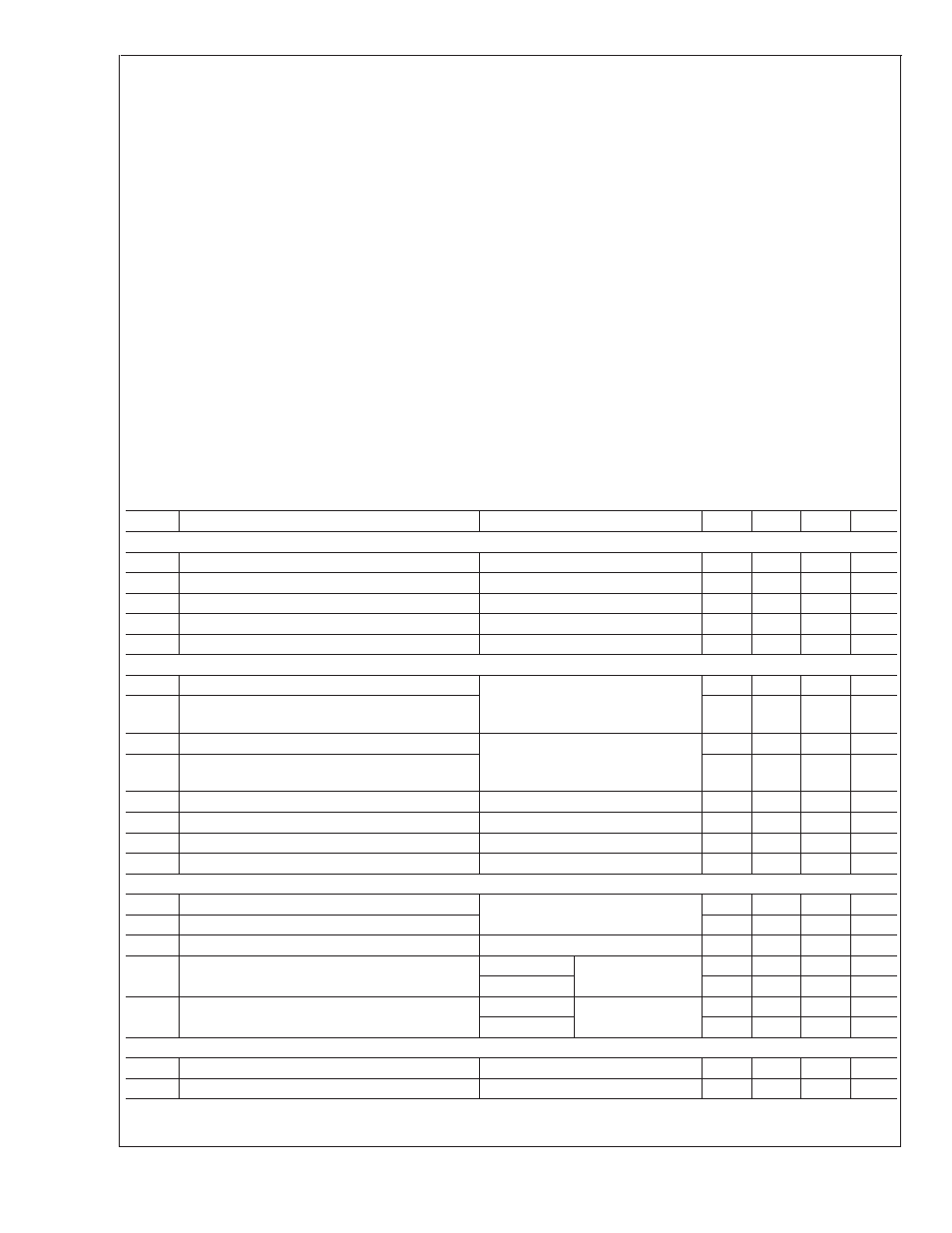
Absolute Maximum Ratings
(Note 1)
If Military/Aerospace specified devices are required,
please contact the National Semiconductor Sales Office/
Distributors for availability and specifications.
Supply Voltage (V
CC
)
−0.3V to +4V
LVCMOS/LVTTL Input Voltage
(EN)
−0.3V to (V
CC
+ 0.3V)
LVDS Receiver Input Voltage
(IN+, IN−)
−0.3V to +4V
LVDS Driver Output Voltage
(OUT+, OUT−)
−0.3V to +4V
LVDS Output Short Circuit
Current
Continuous
Junction Temperature
+150˚C
Storage Temperature Range
−65˚C to +150˚C
Lead Temperature Range
Soldering (4 sec.)
+260˚C
Maximum Package Power Dissipation at 25˚C
M Package
726 mW
Derate M Package
5.8 mW/˚C above +25˚C
LDA Package
2.44 W
Derate LDA Package
19.49 mW/˚C above
+25˚C
ESD Ratings
(HBM, 1.5k
Ω
, 100pF)
≥
2.5kV
(EIAJ, 0
Ω
, 200pF)
≥
250V
Recommended Operating
Conditions
Min
Typ
Max
Units
Supply Voltage (V
CC
)
3.0
3.3
3.6
V
Receiver Input Voltage
0
V
CC
V
Operating Free Air
Temperature
−40
+25
+85
˚C
Electrical Characteristics
Over recommended operating supply and temperature ranges unless otherwise specified. (Notes 2, 3)
Symbol
Parameter
Conditions
Min
Typ
Max
Units
LVCMOS/LVTTL DC SPECIFICATIONS (EN)
V
IH
High Level Input Voltage
2.0
V
CC
V
V
IL
Low Level Input Voltage
GND
0.8
V
I
IH
High Level Input Current
V
IN
= 3.6V or 2.0V, V
CC
= 3.6V
+7
+20
µA
I
IL
Low Level Input Current
V
IN
= GND or 0.8V, V
CC
= 3.6V
±
1
±
10
µA
V
CL
Input Clamp Voltage
I
CL
= −18 mA
−0.6
−1.5
V
LVDS OUTPUT DC SPECIFICATIONS (OUT)
V
OD
Differential Output Voltage
R
L
= 100
Ω
250
325
450
mV
∆
V
OD
Change in Magnitude of V
OD
for Complimentary
Output States
Figure 1 and Figure 2
20
mV
V
OS
Offset Voltage
R
L
= 100
Ω
1.080
1.19
1.375
V
∆
V
OS
Change in Magnitude of V
OS
for Complimentary
Output States
Figure 1
20
mV
I
OZ
Output TRI-STATE Current
EN = 0V, V
OUT
= V
CC
or GND
±
1
±
10
µA
I
OFF
Power-Off Leakage Current
V
CC
= 0V, V
OUT
= 3.6V or GND
±
1
±
10
µA
I
OS
Output Short Circuit Current (Note 4)
EN = V
CC
, V
OUT+
and V
OUT−
= 0V
−16
−24
mA
I
OSD
Differential Output Short Circuit Current (Note 4)
EN = V
CC
, V
OD
= 0V
−7
−12
mA
LVDS RECEIVER DC SPECIFICATIONS (IN)
V
TH
Differential Input High Threshold
V
CM
= +0.05V, +1.2V or +3.25V
0
+100
mV
V
TL
Differential Input Low Threshold
−100
0
mV
V
CMR
Common Mode Voltage Range
V
ID
= 100mV, V
CC
= 3.3V
0.05
3.25
V
I
IN
Input Current
V
IN
= +3.0V
V
CC
= 3.6V or 0V
±
1
±
10
µA
V
IN
= 0V
±
1
±
10
µA
∆
I
IN
Change in Magnitude of I
IN
V
IN
= +3.0V
V
CC
= 3.6V or 0V
1
6
µA
V
IN
= 0V
1
6
µA
SUPPLY CURRENT
I
CCD
Total Supply Current
EN = V
CC
, R
L
= 100
Ω
, C
L
= 5 pF
47
70
mA
I
CCZ
TRI-STATE Supply Current
EN = 0V
22
35
mA
DS90L
V001
www.national.com
2