Operation, Figure 1. block diagram signal descriptions – Rainbow Electronics DS1306 User Manual
Page 3
DS1306
3 of 21
OPERATION
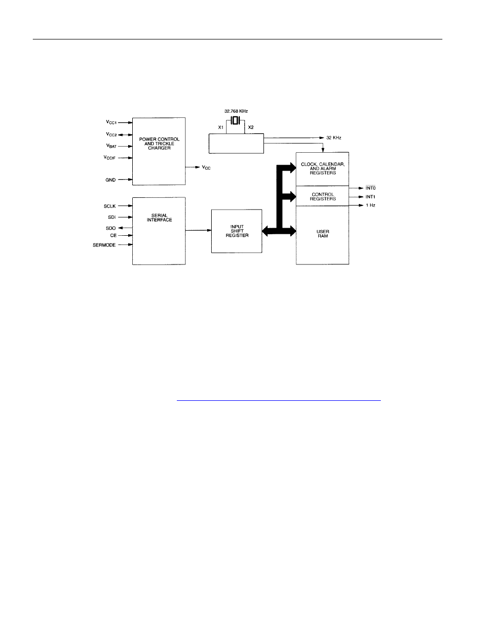
The block diagram in Figure 1 shows the main elements of the serial alarm RTC. The following
paragraphs describe the function of each pin.
Figure 1. BLOCK DIAGRAM
SIGNAL DESCRIPTIONS
V
CC1
– DC power is provided to the device on this pin. V
CC1
is the primary power supply.
V
CC2
– This is the secondary power supply pin. In systems using the trickle charger, the rechargeable
energy source is connected to this pin.
V
BAT
– Battery input for any standard 3V lithium cell or other energy source. UL recognized to ensure
against reverse charging current when used in conjunction with a lithium battery.
See “Conditions of Acceptability”
V
CCIF
(Interface Logic Power Supply Input) – The V
CCIF
pin allows the DS1306 to drive SDO and
32kHz output pins to a level that is compatible with the interface logic, thus allowing an easy interface to
3V logic in mixed supply systems. This pin is physically connected to the source connection of the p-
channel transistors in the output buffers of the SDO and 32kHz pins.
SERMODE (Serial Interface Mode Input) – The SERMODE pin offers the flexibility to choose
between two serial interface modes. When connected to GND, standard 3-wire communication is
selected. When connected to V
CC
, SPI communication is selected.
SCLK (Serial Clock Input) – SCLK is used to synchronize data movement on the serial interface for
either the SPI or 3-wire interface.
SDI (Serial Data Input) – When SPI communication is selected, the SDI pin is the serial data input for
the SPI bus. When 3-wire communication is selected, this pin must be tied to the SDO pin (the SDI and
SDO pins function as a single I/O pin when tied together).
OSCILLATOR AND
COUNTDOWN CHAIN
1Hz