Rainbow Electronics DS1306 User Manual
Page 13
DS1306
13 of 21
The address byte is always the first byte entered after CE is driven high. The most significant bit (A7) of
this byte determines if a read or write takes place. If A7 is 0, one or more read cycles occur. If A7 is 1,
one or more write cycles occur.
Data transfers can occur one byte at a time or in multiple-byte burst mode. After CE is driven high an
address is written to the DS1306. After the address, 1 or more data bytes can be written or read. For a
single-byte transfer, one byte is read or written and then CE is driven low. For a multiple-byte transfer,
however, multiple bytes can be read or written to the DS1306 after the address has been written. Each
read or write cycle causes the RTC register or RAM address to automatically increment. Incrementing
continues until the device is disabled. When the RTC is selected, the address wraps to 00h after
incrementing to 1Fh (during a read) and wraps to 80h after incrementing to 9Fh (during a write). When
the RAM is selected, the address wraps to 20h after incrementing to 7Fh (during a read) and wraps to
A0h after incrementing to FFh (during a write).
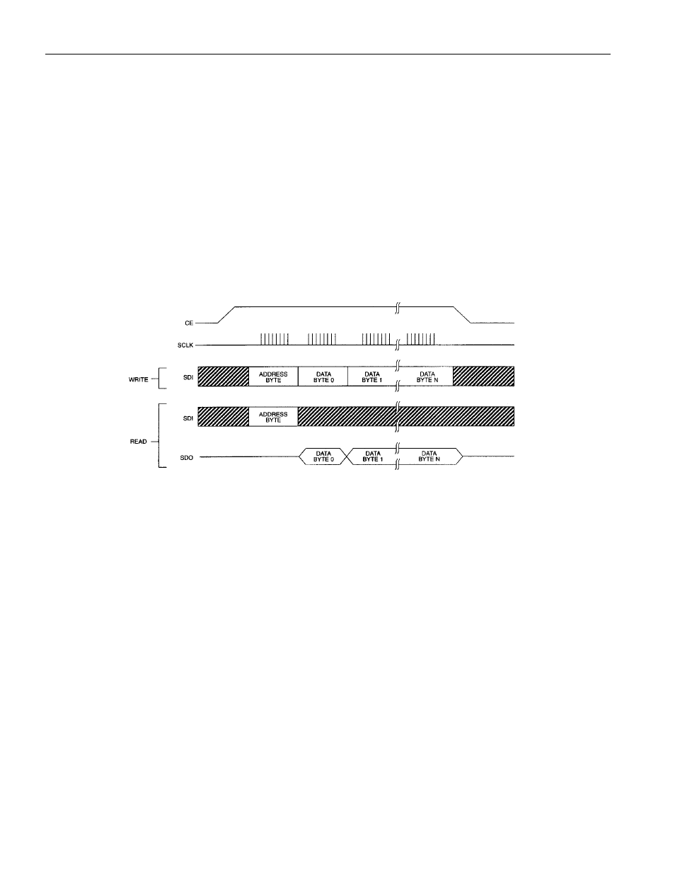
Figure 8. SPI MULTIPLE-BYTE BURST TRANSFER
READING AND WRITING IN BURST MODE
Burst mode is similar to a single-byte read or write, except that CE is kept high and additional SCLK
cycles are sent until the end of the burst. The clock registers and the user RAM may be read or written in
burst mode. When accessing the clock registers in burst mode, the address pointer will wrap around after
reaching 1Fh (9Fh for writes). When accessing the user RAM in burst mode, the address pointer wraps
around after reaching 7Fh (FFh for writes).