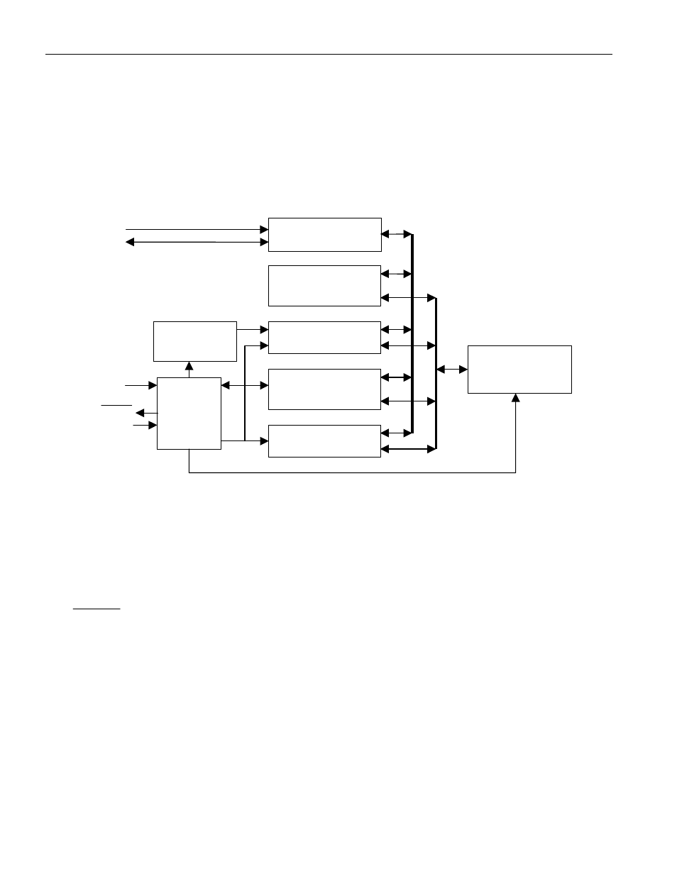
Operation, Figure 1. block diagram – Rainbow Electronics DS1682 User Manual
Page 2

DS1682
2 of 15
OPERATION
The block diagram in Figure 1 shows the relationship between the major functional blocks, the serial
interface, and the EEPROM memory section of the DS1682. Upon power-up, the DS1682 transfers the
contents of the EEPROM into the counters and memory registers where the data can be read and written
through the serial interface. The content of the counters and memory registers are written into the
EEPROM memory when the EVENT pin transitions from a logic high to a logic low.
Figure 1. BLOCK DIAGRAM
The DS1682 uses a calibrated, temperature-compensated RC time base to increment an elapsed time
counter (ETC) while an event is active. When the event becomes active, the contents of the nonvolatile
EEPROM are transferred to the ETC and event counter and the oscillator starts. As the event continues,
the ETC is incremented in quarter-second increments. When the event becomes inactive, the event
counter is incremented and the contents of the ETC and event counter are written to the nonvolatile
EEPROM.
The ALARM output can be used to indicate when the ETC has matched the value in the alarm register.
The DS1682 can be configured to prevent clearing the alarm and the elapsed time and event counters.
The user memory can be separately write-protected.
OSCILLATOR
AND
DIVIDER
CONTROL
LOGIC
AND
EVENT
GLITCH
FILTER
EVENT COUNTER
SERIAL
INTERFACE
USER, CONTROL, AND
CONFIGURATION
REGISTERS
EVENT
SDA
SCL
ALARM
ALARM REGS
AND
COMPARE LOGIC
ELAPSED TIME
COUNTER (ETC)
EEPROM ARRAY
V
CC
