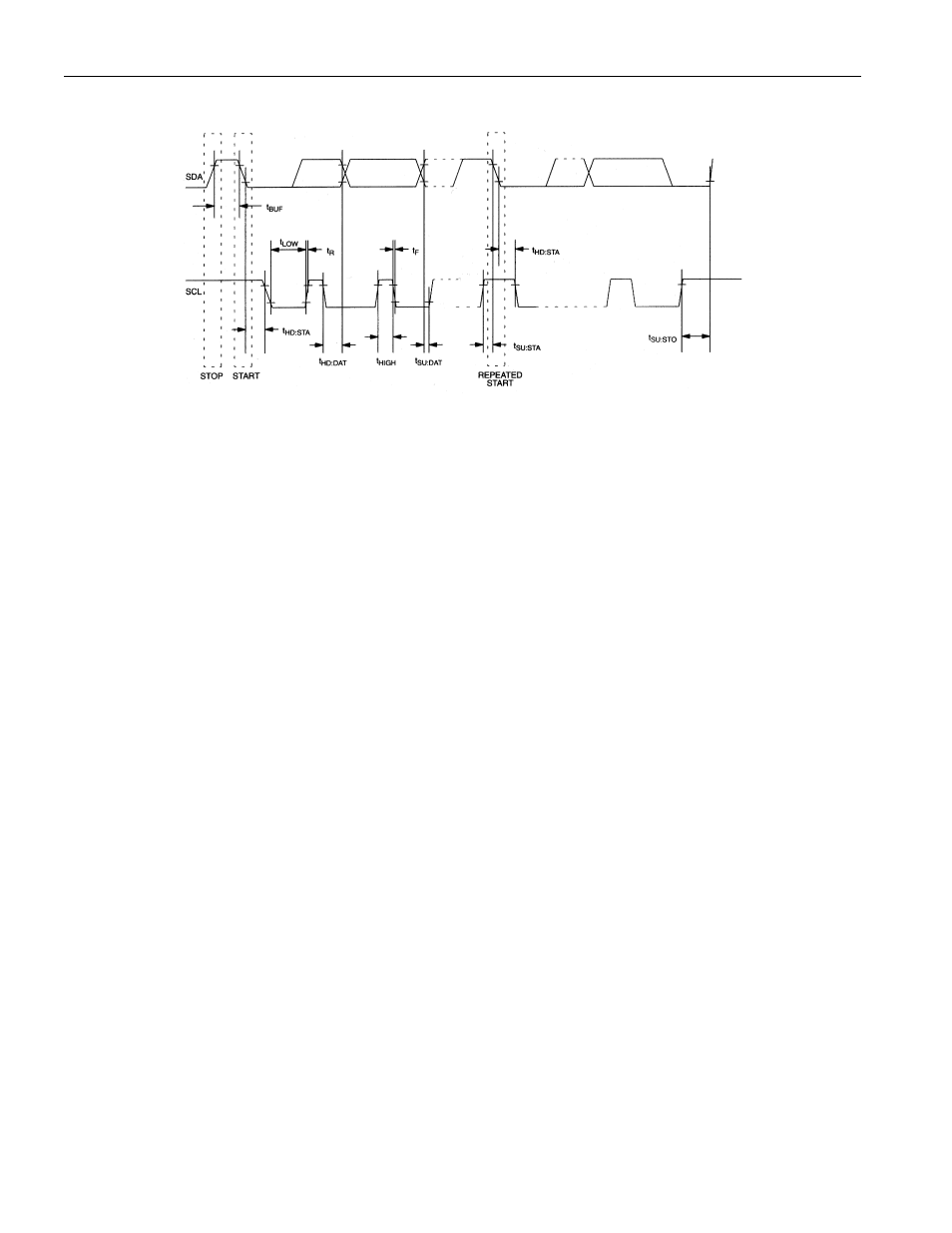
Figure 7. timing diagram – Rainbow Electronics DS1682 User Manual
Page 13

DS1682
13 of 15
Figure 7. TIMING DIAGRAM
NOTES:
1) V
CC
must be at or above 2.5V for t
EW
after the end of an event to insure data transfer to the EEPROM.
2) The elapsed time and event counters are backed by three EEPROM arrays which are used
sequentially, allowing up to 3 x E
E
. The configuration register, alarm trip-point register and user
memory use a single array, limiting them to one E
E
.
3) A decoupling capacitor to supply high instantaneous currents during EEPROM writes is
recommended. A typical value is 0.01µF. V
CC
must be maintained above Vcc minimum, including
transients, during EEPROM writes.
4) Typical values are at +25°C, V
CC
= 4.0V.
5) Reading data while the contents of EEPROM are transferred to RAM results in incorrect reads.
6) After this period, the first clock pulse is generated.
7) A device must internally provide a hold time of at least 300ns for the SDA signal (referred to the
V
IHMIN
of the SCL signal) in order to bridge the undefined region of the falling edge of SCL.
8) The maximum t
HD:DAT
has only to be met if the device does not stretch the low period (t
LOW
) of the
SCL signal.
9) C
B
–Total capacitance of one bus line in pF.
10) A fast-mode device can be used in a standard-mode system, but the requirement t
SU:DAT
≥ 250ns must
be met. This is automatically the case if the device does not stretch the t
LOW
. If such a device does
stretch t
LOW
, it must output the next data bit to the SDA line t
R
max + t
SU:DAT
= 1000 + 250 = 1250ns
before the SCL line is released.
