I/o signaling, Write-time slots, Read-time slots – Rainbow Electronics DS25LV02 User Manual
Page 11: Figure 5. 1-wire initialization sequence
DS25LV02: Low-Voltage 1024-Bit EPROM
11 of 17
step routine: read a bit, read the complement of the bit, then write the desired value of that bit. The bus master
performs this simple three-step routine on each bit location of the net address. After one complete pass through all
64 bits, the bus master knows the address of one device. The remaining devices can then be identified on
additional iterations of the process. Refer to Chapter 5 of the Book of DS19xx iButton Standards for a
comprehensive discussion of a net address search, including an actual example (
www.maxim-ic.com/iButtonBook
).
I/O SIGNALING
The 1-Wire bus requires strict signaling protocols to ensure data integrity. The four protocols used by the
DS25LV02 are as follows: the initialization sequence (reset pulse followed by presence pulse), write 0, write 1, and
read data. The bus master initiates all these types of signaling except the presence pulse.
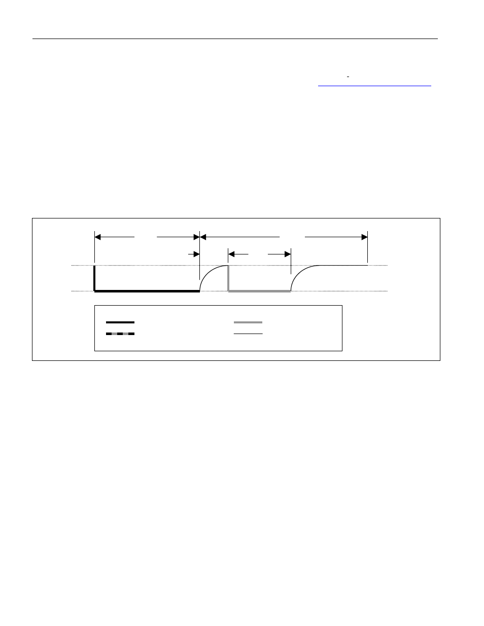
The initialization sequence required to begin any communication with the DS25LV02 is shown in Figure 5. A
presence pulse following a reset pulse indicates that the DS25LV02 is ready to accept a net address command.
The bus master transmits (Tx) a reset pulse for t
RSTL
. The bus master then releases the line and goes into receive
mode (Rx). The 1-Wire bus line is then pulled high by the pullup resistor. After detecting the rising edge on the DQ
pin, the DS25LV02 waits for t
PDH
and then transmits the presence pulse for t
PDL
.
Figure 5. 1-Wire Initialization Sequence
WRITE-TIME SLOTS
A write-time slot is initiated when the bus master pulls the 1-Wire bus from a logic-high (inactive) level to a logic-low
level. There are two types of write-time slots: write 1 and write 0. All write-time slots must be t
SLOT
in duration with
a 1
ms minimum recovery time, t
REC
, between cycles. The DS25LV02 samples the 1-Wire bus line between t
LOW1_MAX
and t
LOW0_MIN
after the line falls. If the line is high when sampled, a write 1 occurs. If the line is low when sampled, a
write 0 occurs. The sample window is illustrated in Figure 6. For the bus master to generate a write-1 time slot, the
bus line must be pulled low and then released, allowing the line to be pulled high less than t
RDV
after the start of the
write time slot. For the host to generate a write-0 time slot, the bus line must be pulled low and held low for the
duration of the write-time slot.
READ-TIME SLOTS
A read-time slot is initiated when the bus master pulls the 1-Wire bus line from a logic-high level to a logic-low level.
The bus master must keep the bus line low for at least 1
ms and then release it to allow the DS25LV02 to present
valid data. The bus master can then sample the data t
RDV
from the start of the read-time slot. By the end of the
read-time slot, the DS25LV02 releases the bus line and allows it to be pulled high by the external pullup resistor. All
read-time slots must be t
SLOT
in duration with a 1
ms minimum recovery time, t
REC
, between cycles. See Figure 6 and
the timing specifications in the Electrical Characteristics table for more information.
t
RSTL
t
PDL
t
RSTH
t
PDH
PACK+
PACK-
LINE TYPE LEGEND:
BUS MASTER ACTIVE LOW
SLAVE ACTIVE LOW
RESISTOR PULLUP
BOTH BUS MASTER AND
SLAVE ACTIVE LOW
DQ