Time chip comparison register definition figure 2, Nonvolatile controller operation – Rainbow Electronics DS1315 User Manual
Page 4
DS1315
041697 4/22
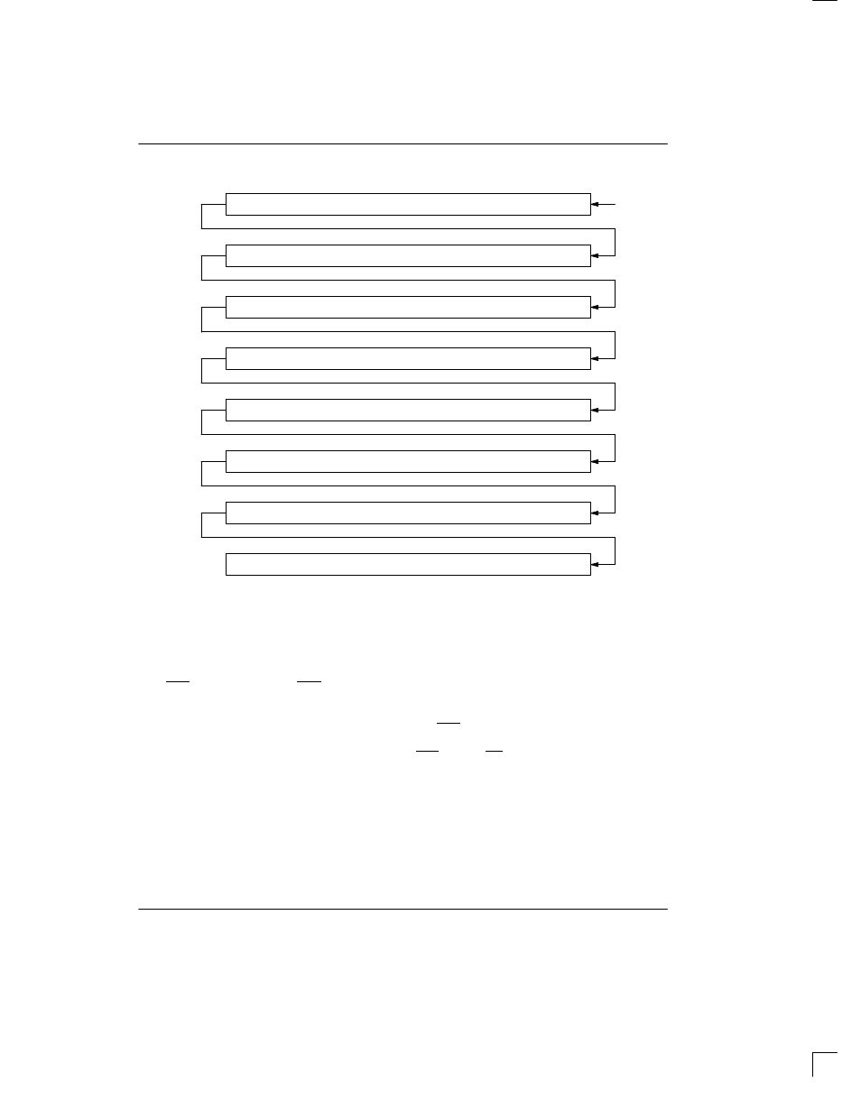
TIME CHIP COMPARISON REGISTER DEFINITION Figure 2
7
6
5
4
3
2
1
0
1
1
0
0
0
1
0
1
0
0
1
1
1
0
1
0
1
0
1
0
0
0
1
1
0
1
0
1
1
1
0
0
1
1
0
0
0
1
0
1
0
0
1
1
1
0
1
0
1
0
1
0
0
0
1
1
0
1
0
1
1
1
0
0
C5
3A
A3
5C
C5
3A
A3
5C
BYTE 0
BYTE 1
BYTE 2
BYTE 3
BYTE 4
BYTE 5
BYTE 6
BYTE 7
NOTE:
The pattern recognition in Hex is C5, 3A, A3, 5C, C5, 3A, A3, 5C. The odds of this pattern being accidentally duplicated
and causing inadvertent entry to the Phantom Time Chip are less than 1 in 10
19
.
NONVOLATILE CONTROLLER OPERATION
The operation of the nonvolatile controller circuits within
the Time Chip is determined by the level of the
ROM/RAM select pin. When ROM/RAM is connected to
ground, the controller is set in the RAM mode and per-
forms the circuit functions required to make CMOS RAM
and the timekeeping function nonvolatile. A switch is
provided to direct power from the battery inputs or V
CCI
to V
CCO
with a maximum voltage drop of 0.3 volts. The
V
CCO
output pin is used to supply uninterrupted power
to CMOS SRAM. The DS1315 also performs redundant
battery control for high reliability. On power–fail, the bat-
tery with the highest voltage is automatically switched to
V
CCO
. If only one battery is used in the system, the un-
used battery input should be connected to ground.
The DS1315 safeguards the Time Chip and RAM data
by power–fail detection and write protection. Power–fail
detection occurs when V
CCI
falls below V
PF
which is set
by an internal bandgap reference. The DS1315 con-
stantly monitors the V
CCI
supply pin. When V
CCI
is less
than V
PF
, power–fail circuitry forces the chip enable out-
put (CEO) to V
CCI
or V
BAT
–0.2 volts for external RAM
write protection. During nominal supply conditions,
CEO will track CEI with a maximum propagation delay
of 5 ns. Internally, the DS1315 aborts any data transfer
in progress without changing any of the Time Chip regis-
ters and prevents future access until V
CCI
exceeds V
PF
.
A typical RAM/Time Chip interface is illustrated in
Figure 3.