Pin description, Description, Operation – Rainbow Electronics DS1315 User Manual
Page 2: Timing block diagram figure 1
DS1315
041697 2/22
PIN DESCRIPTION
X1, X2
– 32.768 KHz Crystal Connection
WE
– Write Enable
BAT1
– Battery 1 Input
GND
– Ground
D
– Data Input
Q
– Data Output
ROM/RAM
– ROM/RAM Mode Select
CEO
– Chip Enable Output
CEI
– Chip Enable Input
OE
– Output Enable
RST
– Reset
BAT2
– Battery 2 Input
V
CCO
– Switched Supply Output
V
CCI
– Power Supply Input
DESCRIPTION
The DS1315 Phantom Time Chip is a combination of a
CMOS timekeeper and a nonvolatile memory controller.
In the absence of power, an external battery maintains
the timekeeping operation and provides power for a
CMOS static RAM. The watch keeps track of hun-
dredths of seconds, seconds, minutes, hours, day, date,
month, and year information. The last day of the month
is automatically adjusted for months with less than
31 days, including leap year correction. The watch oper-
ates in one of two formats: a 12–hour mode with an
AM/PM indicator or a 24–hour mode. The nonvolatile
controller supplies all the necessary support circuitry to
convert a CMOS RAM to a nonvolatile memory. The
DS1315 can be interfaced with either RAM or ROM
without leaving gaps in memory.
OPERATION
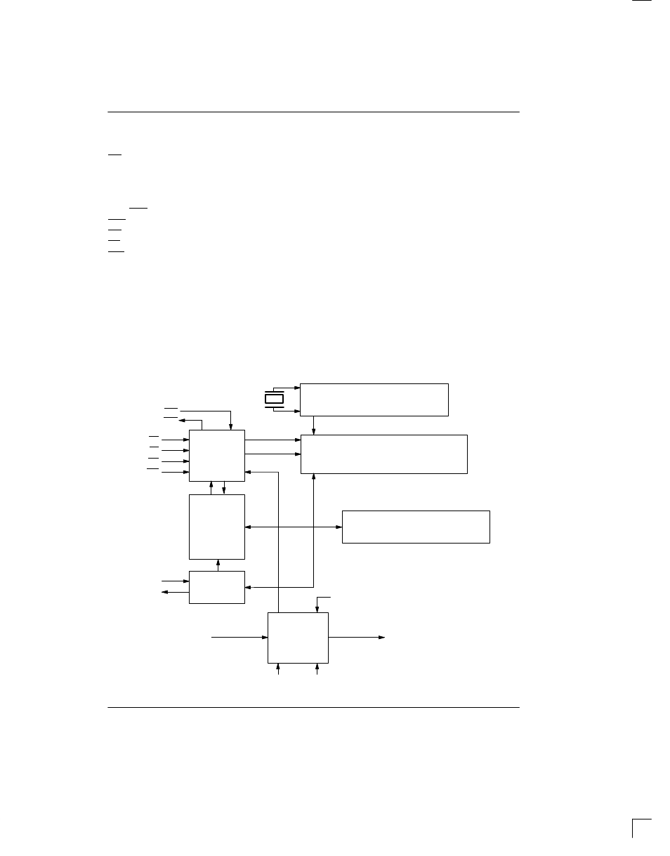
The block diagram of Figure 1 illustrates the main ele-
ments of the Time Chip. The following paragraphs
describe the signals and functions.
TIMING BLOCK DIAGRAM Figure 1
CLOCK/CALENDAR LOGIC
UPDATE
TIMEKEEPING REGISTER
COMPARISON REGISTER
INTERNAL V
CC
V
CCO
V
CCI
X
1
X
2
D
Q
DATA
POWER–FAIL
WRITE
READ
CEO
ROM/RAM
BAT
1
BAT
2
32.768 KHz
CEI
OE
WE
RST
CONTROL
LOGIC
ACCESS
ENABLE
SEQUENCE
DETECTOR
I/O BUFFERS
POWER–FAIL
DETECT
LOGIC