Absolute maximum ratings, Recommended operating conditions, Dc electrical characteristics – Rainbow Electronics DS92LV040A User Manual
Page 2
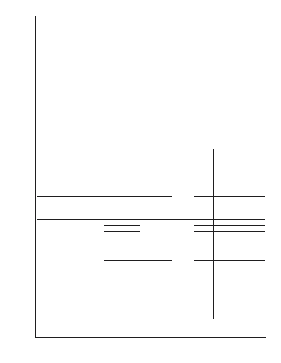
Absolute Maximum Ratings
(Notes 1,
If Military/Aerospace specified devices are required,
please contact the National Semiconductor Sales Office/
Distributors for availability and specifications.
Supply Voltage (V
CC
)
4.0V
Enable Input Voltage
(DE, RE)
−0.3V to (V
CC
+0.3V)
Driver Input Voltage (D
IN
)
−0.3V to (V
CC
+0.3V)
Receiver Output Voltage
(R
OUT
)
−0.3V to (V
CC
+0.3V)
Bus Pin Voltage (DO/RI
±
)
−0.3V to +3.9V
ESD (Note 4)
(HBM 1.5 k
Ω, 100 pF)
>
4kV
Machine Model
>
250V
Maximum Package Power Dissipation at 25˚C
4.8 W
Derate LLP Package
38.8mW/˚C
θ
ja
25.8˚C/W
θ
jc
25.5˚C/W
Storage Temperature Range
−65˚C to +150˚C
Lead Temperature
(Soldering, 4 sec.)
260˚C
Recommended Operating
Conditions
Min
Max
Units
Supply Voltage (V
CC
)
3.0
3.6
V
Receiver Input Voltage
0.0
2.4
V
Operating Free Air Temperature
−40
+85
˚C
Slowest Input Edge Rate
(Note 7)(20% to 80%)
∆t/∆V
Data
1.0
ns/V
Control
3.0
ns/V
DC Electrical Characteristics
Over recommended operating supply voltage and temperature ranges unless otherwise specified (Notes 2, 4)
Symbol
Parameter
Conditions
Pin
Min
Typ
Max
Units
V
OD
Output Differential
Voltage
R
L
= 27
Ω, Figure 1
DO+/RI+,
DO−/RI−
200
300
460
mV
∆V
OD
V
OD
Magnitude Change
5
27
mV
V
OS
Offset Voltage
1.1
1.3
1.5
V
∆V
OS
Offset Magnitude Change
5
10
mV
V
OHD
Driver Output High
Voltage
R
L
= 27
Ω
1.4
1.65
V
V
OLD
Driver Output Low
Voltage
R
L
= 27
Ω
0.95
1.1
V
I
OSD
Driver Output Short
Circuit Current (Note 11)
V
OD
= 0V, DE = V
CC
, Driver outputs
shorted together
|30|
| 45|
mA
V
OHR
Receiver Voltage Output
High (Note 12)
V
ID
= +300 mV
I
OH
= −4 mA
R
OUT
V
CC
−0.2
V
Inputs Open
V
CC
−0.2
V
Inputs Terminated,
R
L
= 27
Ω
V
CC
−0.2
V
V
OLR
Receiver Voltage Output
Low
I
OL
= 4.0 mA, V
ID
= −300 mV
0.05
0.100
V
I
OD
Receiver Output Dynamic
Current (Note 11)
V
ID
= 300mV, V
OUT
= V
CC
−1.0V
−50
|33|
mA
V
ID
= −300mV, V
OUT
= 1.0V
|36|
60
mA
V
TH
Input Threshold High
DE = 0V, Over common mode range
DO+/RI+,
DO−/RI−
−40
0
mV
V
TL
Input Threshold Low
−70
−40
mV
V
CMR
Receiver Common Mode
Range
|V
ID
|/2
2.4 −
|V
ID
|/2
V
I
IN
Input Current
DE = 0V, RE = 2.4V,
V
IN
= +2.4V or 0V
−20
±
1
+20
µA
V
CC
= 0V, V
IN
= +2.4V or 0V
−20
±
1
+20
µA
DS92L
V040A
www.national.com
2