Ds4266 ddr clock oscillator, Detailed description, Additional information – Rainbow Electronics DS4266 User Manual
Page 5
DS4266
DDR Clock Oscillator
_______________________________________________________________________________________
5
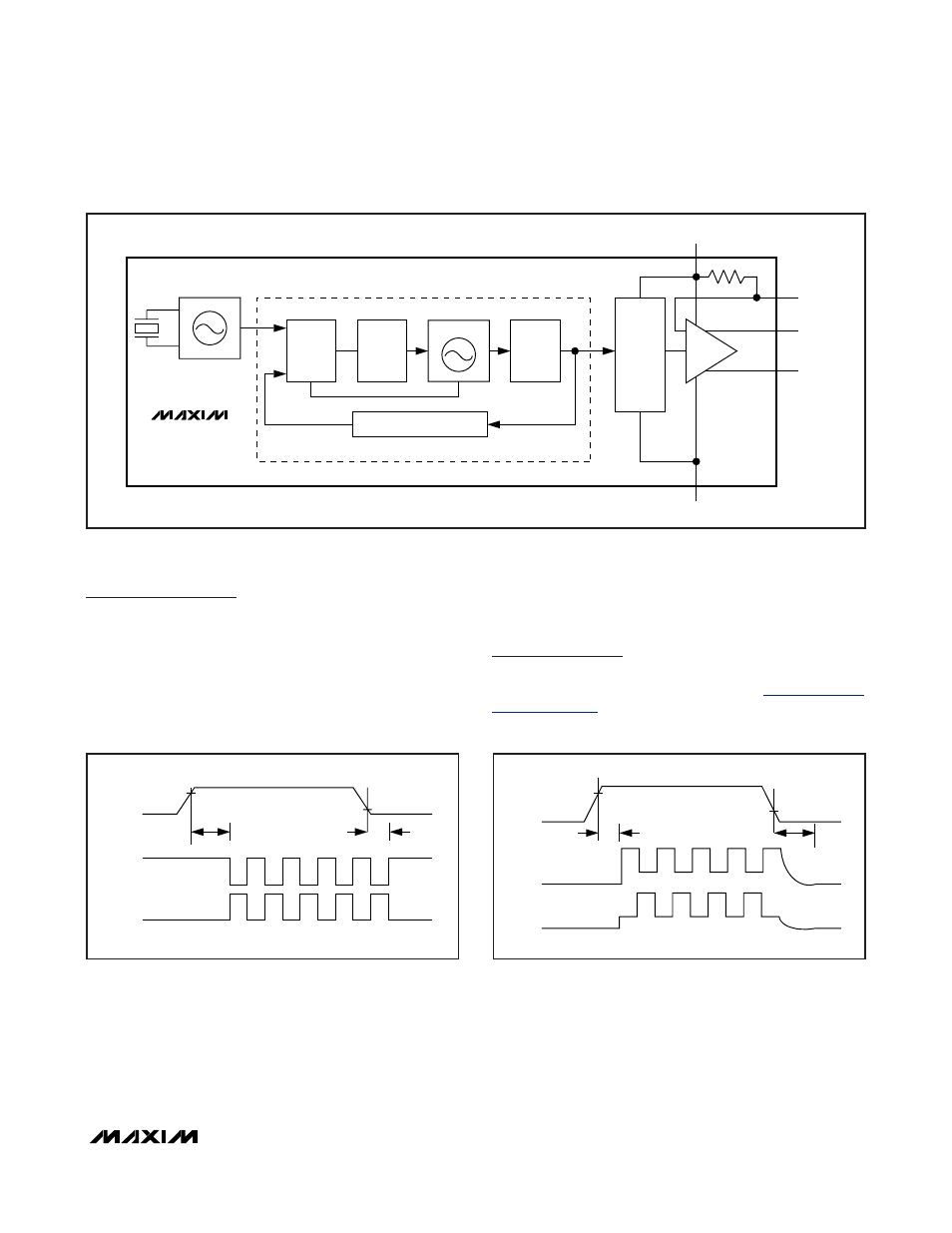
Detailed Description
The DS4266 consists of a fundamental-mode crystal
and synthesizer IC packaged in a 5mm x 3.2mm x
1.49mm, 10-pin LCCC ceramic package. The device
produces a frequency output of 266.00MHz. Two differ-
ential output types are available: LVDS and LVPECL.
The device output can be enabled or disabled through
the OE signal input. When the OE signal is low, LVPECL
outputs go to the PECL_BAS level of V
CC
- 2.9V, while
the LVDS outputs are a logical 1. See Figures 2 and 3
for LVDS and LVPECL output timing diagrams.
Additional Information
For more available frequencies in the DS4-XO family,
refer to the DS4125 data sheet at
www.maxim-
ic.com/DS4125
.
X1
X2
THREE-
STATE
PHASE
DET
FILTER
LC-VCO
/n
OUTSELN
/m
OUTDRV
V
CC
GND
OE
OUTP
OUTN
DS4266
Figure 1. Functional Diagram
OE
OUTP
t
P1A
t
PA1
0.7 x V
CC
0.3 x V
CC
OUTN
Figure 2. LVDS Output Timing Diagram When OE Is Enabled
and Disabled
OE
OUTP
PECL_BIAS
PECL_BIAS
PECL_BIAS
PECL_BIAS
OUTN
0.7 x V
CC
0.3 x V
CC
t
PAZ
t
PZA
Figure 3. LVPECL Output Timing Diagram When OE Is Enabled
and Disabled