Ds4266 ddr clock oscillator – Rainbow Electronics DS4266 User Manual
Page 2
DS4266
DDR Clock Oscillator
2
_______________________________________________________________________________________
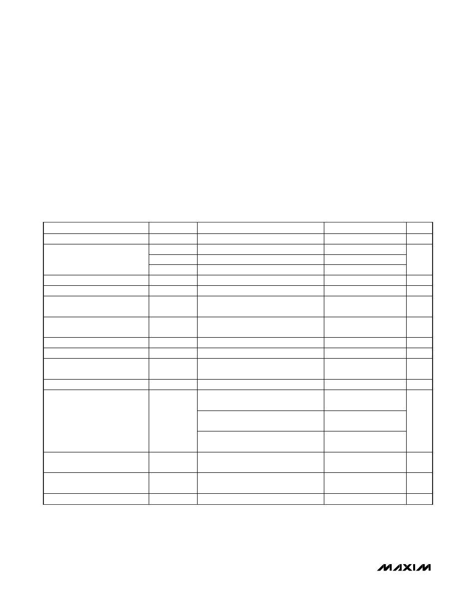
ABSOLUTE MAXIMUM RATINGS
ELECTRICAL CHARACTERISTICS
(V
CC
= 3.135V to 3.465V, T
A
= -40°C to +85°C, unless otherwise noted.)
Stresses beyond those listed under “Absolute Maximum Ratings” may cause permanent damage to the device. These are stress ratings only, and functional
operation of the device at these or any other conditions beyond those indicated in the operational sections of the specifications is not implied. Exposure to
absolute maximum rating conditions for extended periods may affect device reliability.
Power-Supply Voltage (V
CC
) .......................................-0.3V, +4V
Operating Temperature Range ...........................-40
°C to +85°C
Junction Temperature ......................................................+150
°C
Storage Temperature Range ...............................-55
°C to +85°C
Soldering Temperature Profile
(3 passes max of reflow) ......................Refer to the IPC/JEDEC
J-STD-020 Specification.
PARAMETER
SYMBOL
CONDITIONS
MIN
TYP
MAX
UNITS
Operating Voltage Range
V
CC
(Note
1)
3.135
3.3
3.465
V
I
CC_D
LVDS, output loaded or unloaded
52
75
I
CC_PU
LVPECL,
output
unloaded
49 70
Operating Current
I
CC_PI
LVPECL, output load 50
at V
CC
- 2.0V
74
100
mA
Output Frequency
f
OUT
f
NOM
MHz
Oscillator Startup Time
t
STARTUP
(Note
2)
50 ms
Frequency Stability
f
TOTAL
Over temperature range, aging, load,
supply, and initial tolerance (Note 3)
-50 f
NOM
+50 ppm
Frequency Stability Over
Temperature with Initial Tolerance
f
TEMP
V
CC
= 3.3V
-35
+35
ppm
Initial Tolerance
f
INITIAL
V
CC
= 3.3V, T
A
= +25
°C
±20
ppm
Frequency Change Due to
V
CC
f
VCC
V
CC
= 3.3V
±5% -3
+3
ppm/V
Frequency Change Due to Load
Variation
f
LOAD
±10% variation in termination
resistance
±1 ppm
Aging (15 Years)
f
AGING
-7
+7 ppm
Integrated phase RMS; 12kHz to 5MHz,
V
CC
= 3.3V, T
A
= +25
°C
0.7
Integrated phase RMS; 12kHz to 20MHz,
V
CC
= 3.3V, T
A
= +25
°C
0.7
Jitter J
RMS
Integrated phase RMS; 12kHz to 80MHz,
V
CC
= 3.3V, T
A
= +25
°C
1.0
ps
Input-Voltage High (OE)
V
IH
(Note
1)
0.7 x
V
CC
V
CC
V
Input-Voltage Low (OE)
V
IL
(Note
1)
0
0.3 x
V
CC
V
Input Leakage (OE)
I
LEAK
GND
OE V
CC
-50
+5.0
μA