Application information – Rainbow Electronics DS92LV010A User Manual
Page 8
Application Information
(Continued)
•
Bypass each BLVDS device and also use distributed bulk
capacitance. Surface mount capacitors placed close to
power and ground pins work best. Two or three multi-
layer ceramic (MLC) surface mount capacitors (0.1 µF,
and 0.01 µF in parallel should be used between each V
CC
and ground. The capacitors should be as close as pos-
sible to the V
CC
pin.
•
Use the termination resistor which best matches the dif-
ferential impedance of your transmission line.
•
Leave unused LVDS receiver inputs open (floating)
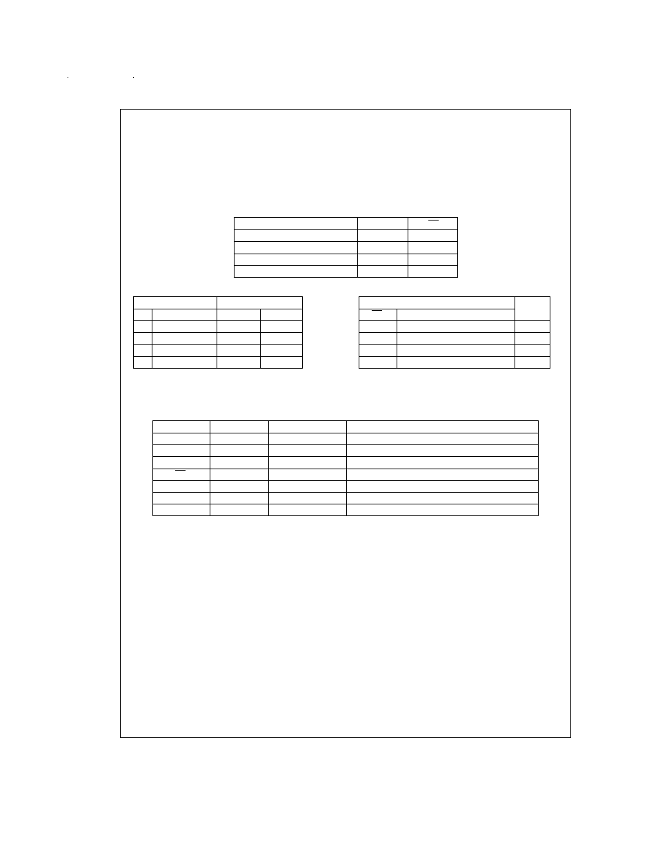
TABLE 1. Functional Table
MODE SELECTED
DE
RE
DRIVER MODE
H
H
RECEIVER MODE
L
L
TRI-STATE MODE
L
H
LOOP BACK MODE
H
L
TABLE 2. Transmitter Mode
INPUTS
OUTPUTS
DE
DI
DO+
DO−
H
L
L
H
H
H
H
L
H
2
>
&
>
0.8
X
X
L
X
Z
Z
L = Low state
H = High state
TABLE 3. Receiver Mode
INPUTS
OUTPUT
RE
(RI+)-(RI−)
L
L (
<
−100 mV)
L
L
H (
>
+100 mV)
H
L
100 mV
>
&
>
−100 mV
X
H
X
Z
X = High or Low logic state
Z = High impedance state
L = Low state
H = High state
TABLE 4. Device Pin Description
Pin Name
Pin #
Input/Output
Description
DIN
2
I
TTL Driver Input
DO
±
/RI
±
6, 7
I/O
LVDS Driver Outputs/LVDS Receiver Inputs
R
OUT
3
O
TTL Receiver Output
RE
5
I
Receiver Enable TTL Input (Active Low)
DE
1
I
Driver Enable TTL Input (Active High)
GND
4
NA
Ground
V
CC
8
NA
Power Supply
www.national.com
8